Silicon Drift Detectors for SEM
IXRF’s range of electronically cooled (LN2 free) Silicon Drift Detectors (SDD) are optimized when coupled with our innovative Ethernet based 550i digital pulse processor. Specifically configured to each customer's scanning electron microscope (SEM), IXRF's SDD detectors provide exceptional and stable performance over a wide range of input count rates to produce rapid X-ray fluorescence elemental maps.
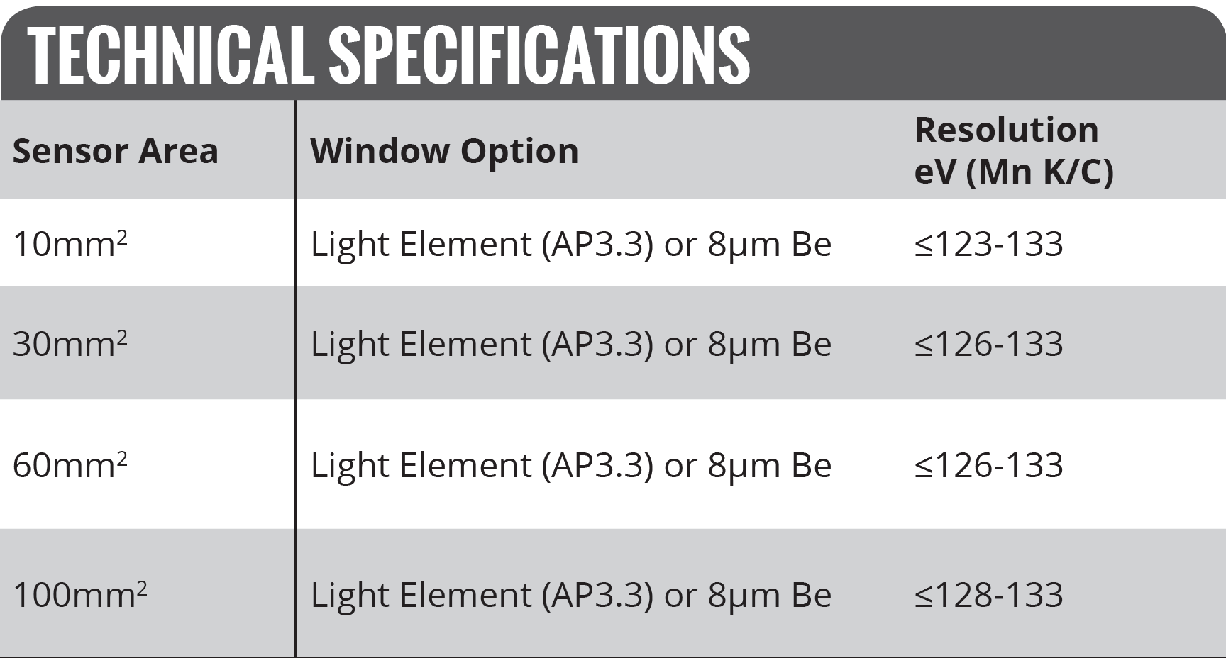
The SDD detector is available in both EDS (SEM mounted with slide assembly) and XRF (various designs, no slide) formats. Choices of window materials are available, from Beryllium (8µm) to Thin Polymer (for light element x-ray transmission) and sensor active areas of 10mm² to 100mm² are offered. In addition, all or our SEM SDD versions are vibration free.
DOWNLOAD DETECTORS FLYERFeatures
IXRF can update your SEM/EDS software and computer to the safety and security of the Windows 10 OS environment. Interoperability with Microsoft Office means generation of reports is simple and intuitive. And your SEM will be compliant with the latest corporate/institutional security protocols.
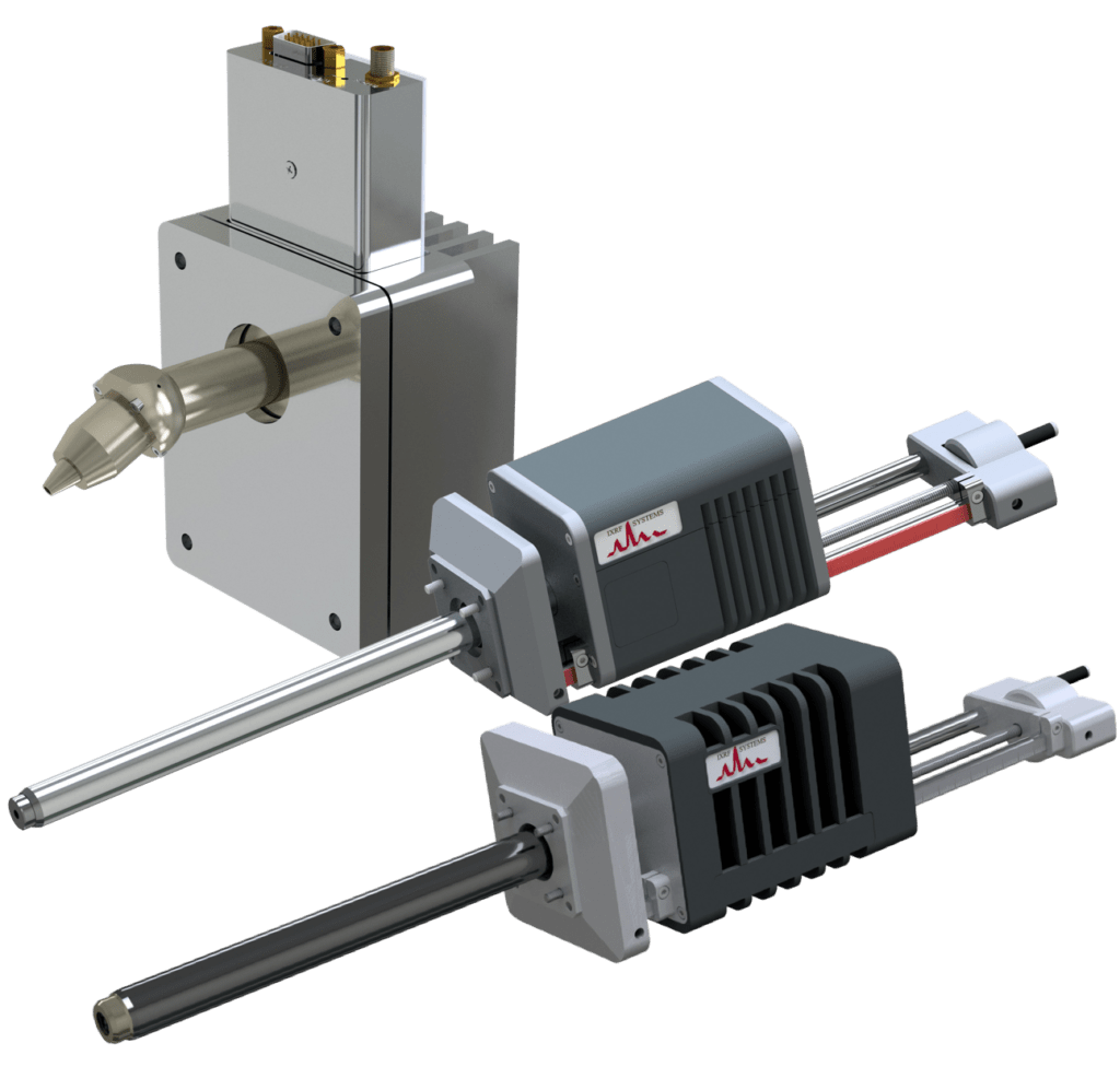
microXRF X-ray sources for Scanning Electron Microscopes (SEM): addition of an polycapillary X-ray tube and Iridium Ultra software will transform your SEM’s quantitative analytical capabilities. Higher peak to background ratios enable greater elemental sensitivity for higher Z elements: sensitivity exceeding e–-beam excitation by a factor of 10-1000X.
ABSTRACT
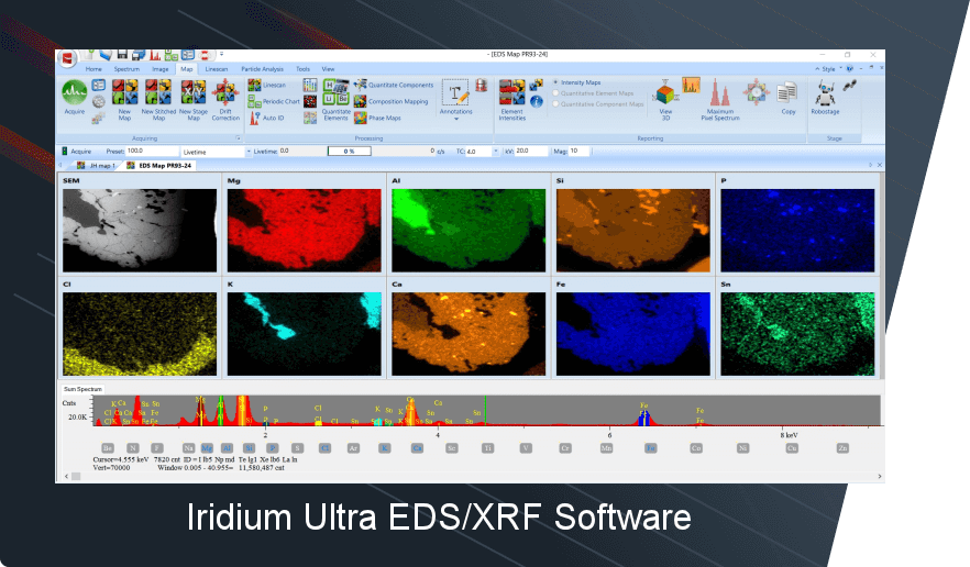
In the 50 years since the first mating of semiconductor-based energy-dispersive X-ray spectrometry (EDS) with the scanning electron microscope (SEM), this hybrid instrument has become an indispensable microanalytical tool. In the last two decades a new detector, the silicon drift detector (SDD), has overtaken earlier Si(Li) technology and has made EDS in the SEM and TEM faster and better. This article tells the story of the SDD development and describes improvements in count rate capability, energy resolution, and detector geometry that bring to SEM microanalysis exceptional precision and stability. Quality maps of element distributions can now be obtained in minutes instead of hours.
Sample Applications
Archeology/Museums
Museum artifacts and currency
Metals and alloys
Gemstone inclusions
Painting authenticity/dating
Paints, inks, pigments
Corrosion products
Biomedical devices/implants
Solar cells
Optical filters
Manufacturing
Pathology
Pharmaceuticals
Semiconductor
RoHS, WEEE, and ELV compliance
Geological
Meteorites
Phase boundaries
Mineral identification
Mining test cores
Electronics
Glasses
Building materials (concrete, cement)
Packaging
Medicine/Biology
Bones/tissue
Leaves/plants
Implants
Particle Analysis
Environmental analysis
Lead contamination in consumer goods
Soil contamination
Material characterization for recycling
Marine/ocean sediments
Airborne particles/air filters
Slurry
Forensic Science
Glass Chips
Paint cross sections
Inks/pigments
Soils/stones
Gun shot residue
Material identification