Micro X-ray Fluorescence (μXRF) Hyperspectral Imaging Elemental Analyzer

ATLAS M : micro XRF Spectrometer

circuit board

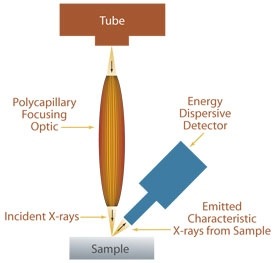
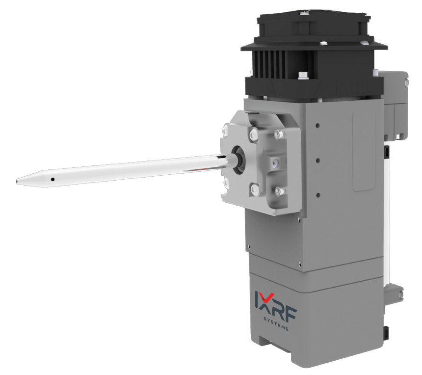
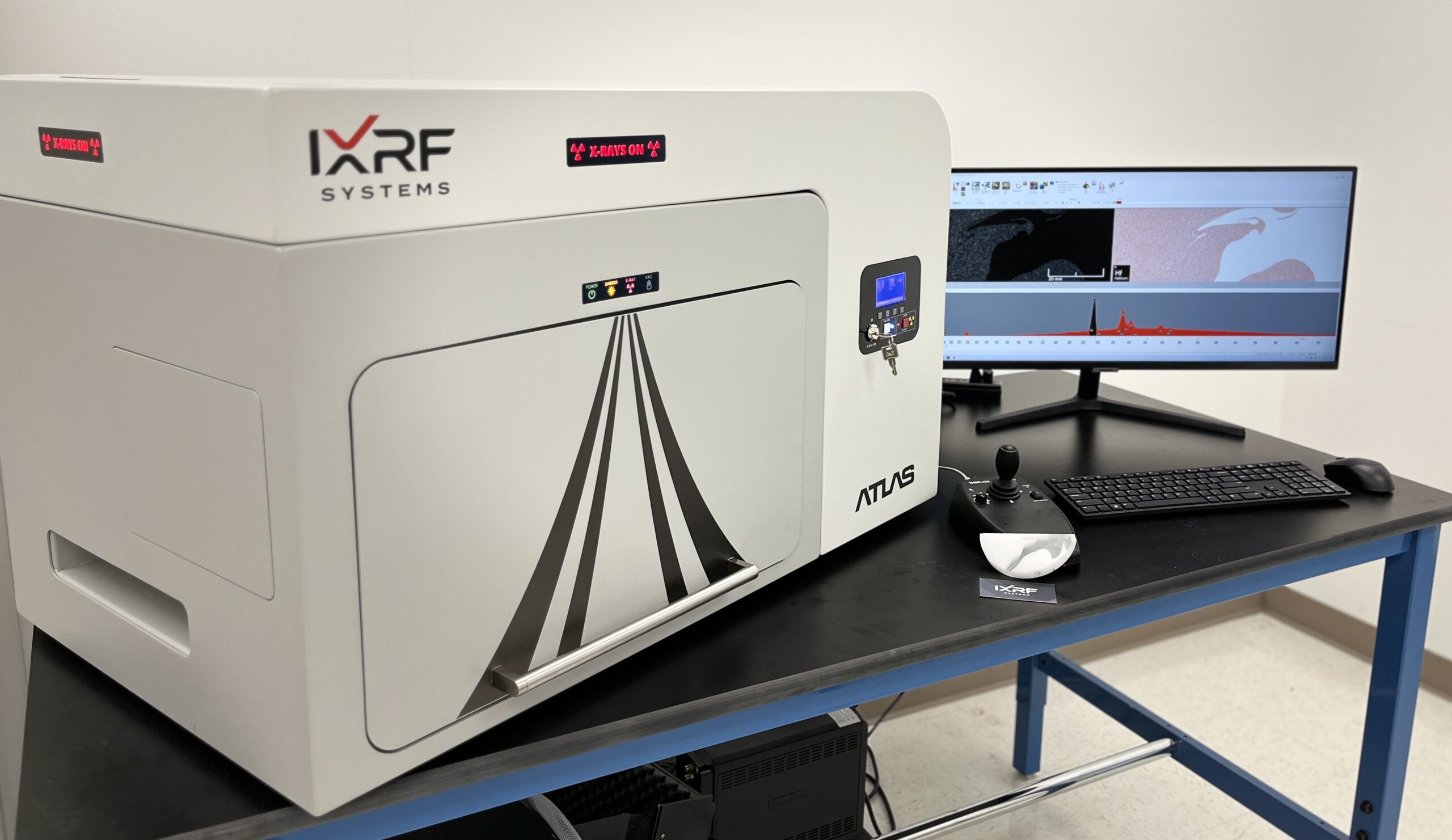
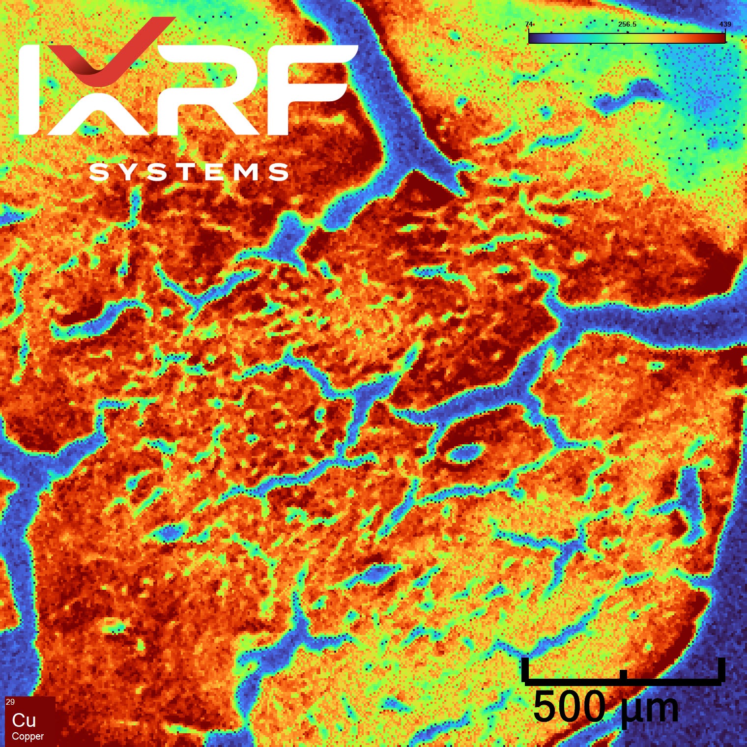
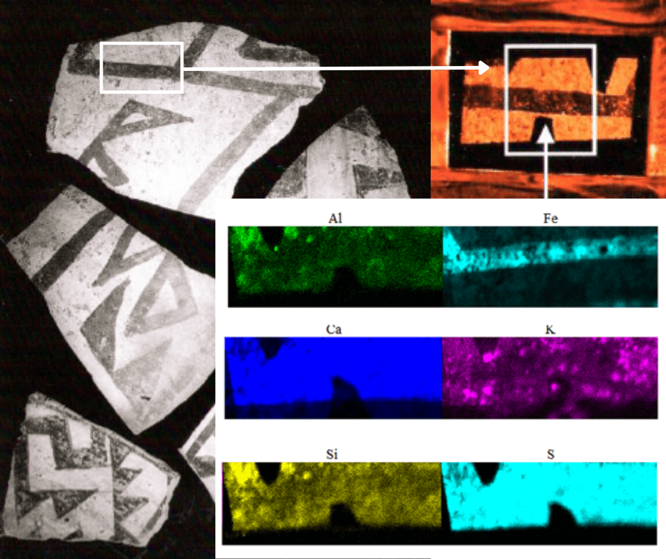
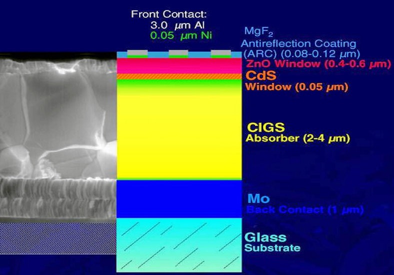
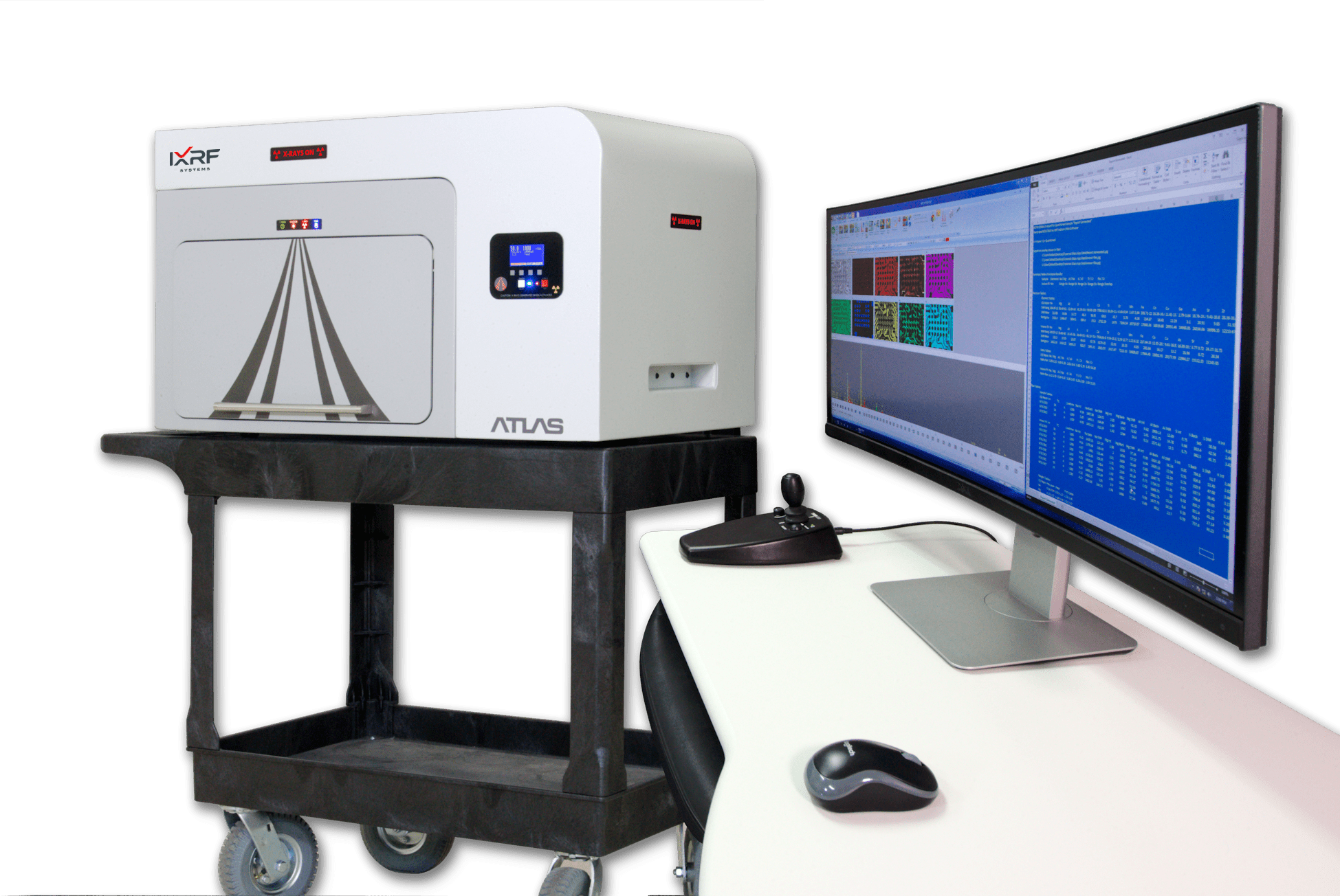
IXRF Systems’ ATLAS M benchtop microEDXRF (micro XRF) spectrometer is the latest general-purpose micro spot energy dispersive X-ray fluorescence (EDXRF) spectrometer microscope for the measurement and mapping of elements from sodium (Na) through uranium (U). Designed to image and analyze a wide variety of sample types, ATLAS leads the industry in virtually every major specification category, from the most powerful software and the highest detector active area to our superior perpendicular (normal) X-ray tube geometry and smallest micro spot.

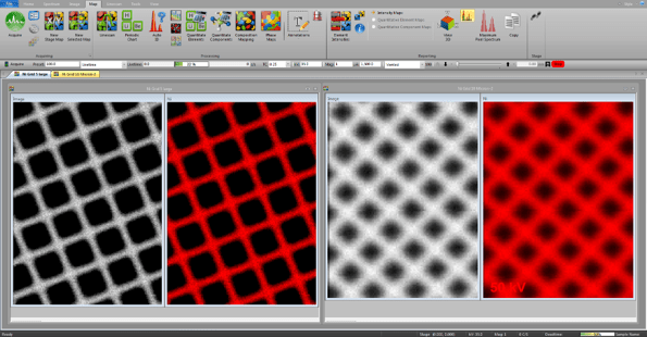
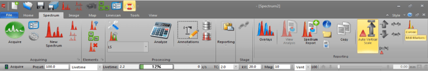
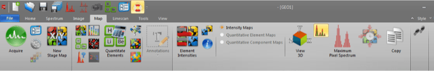
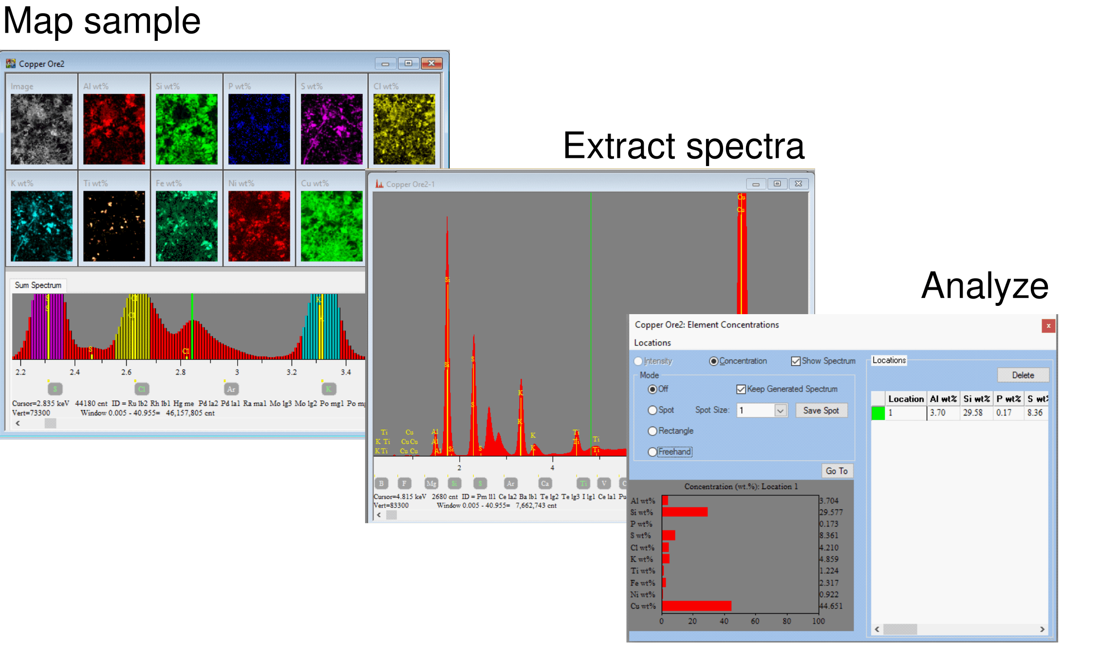
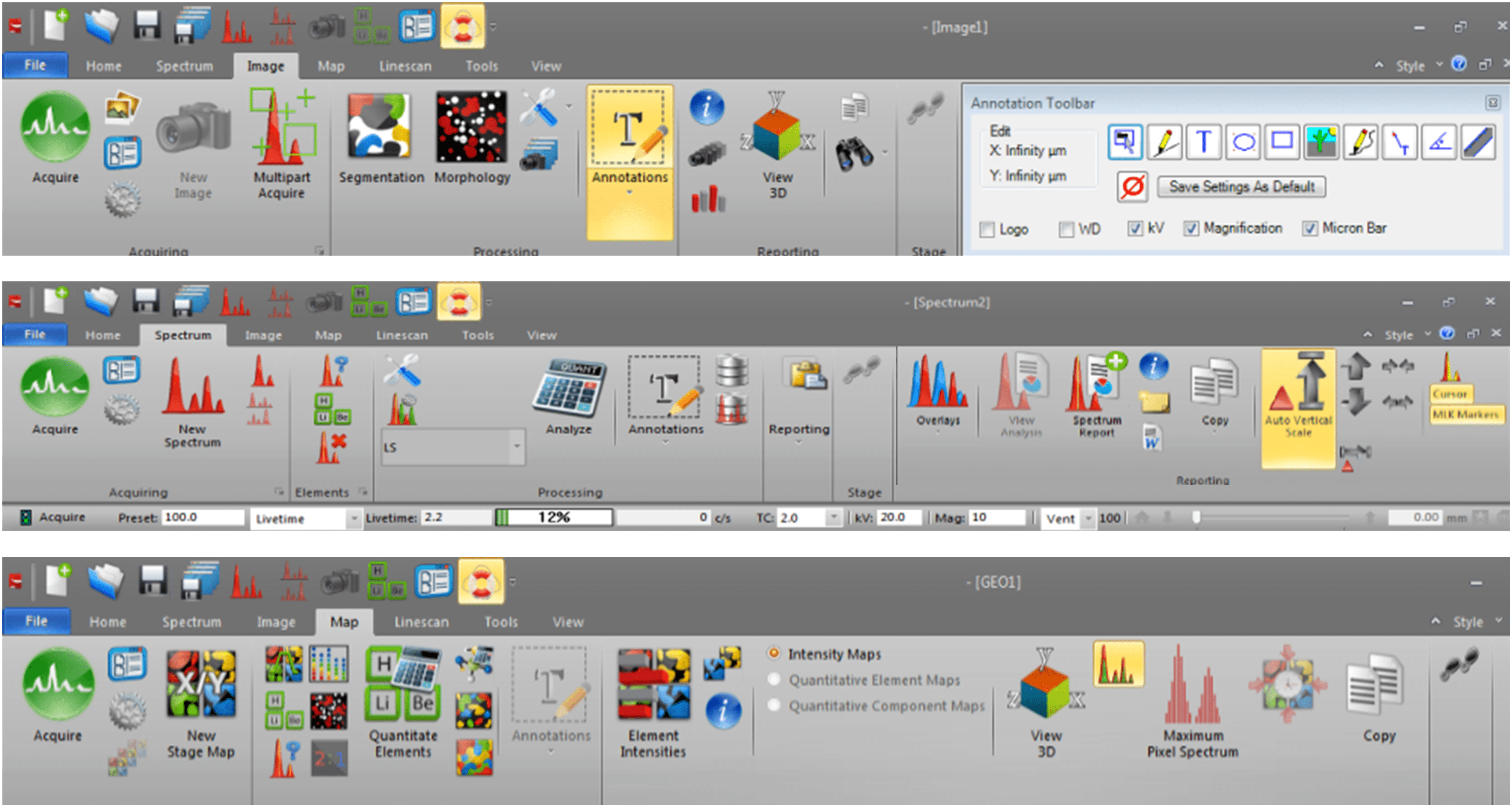
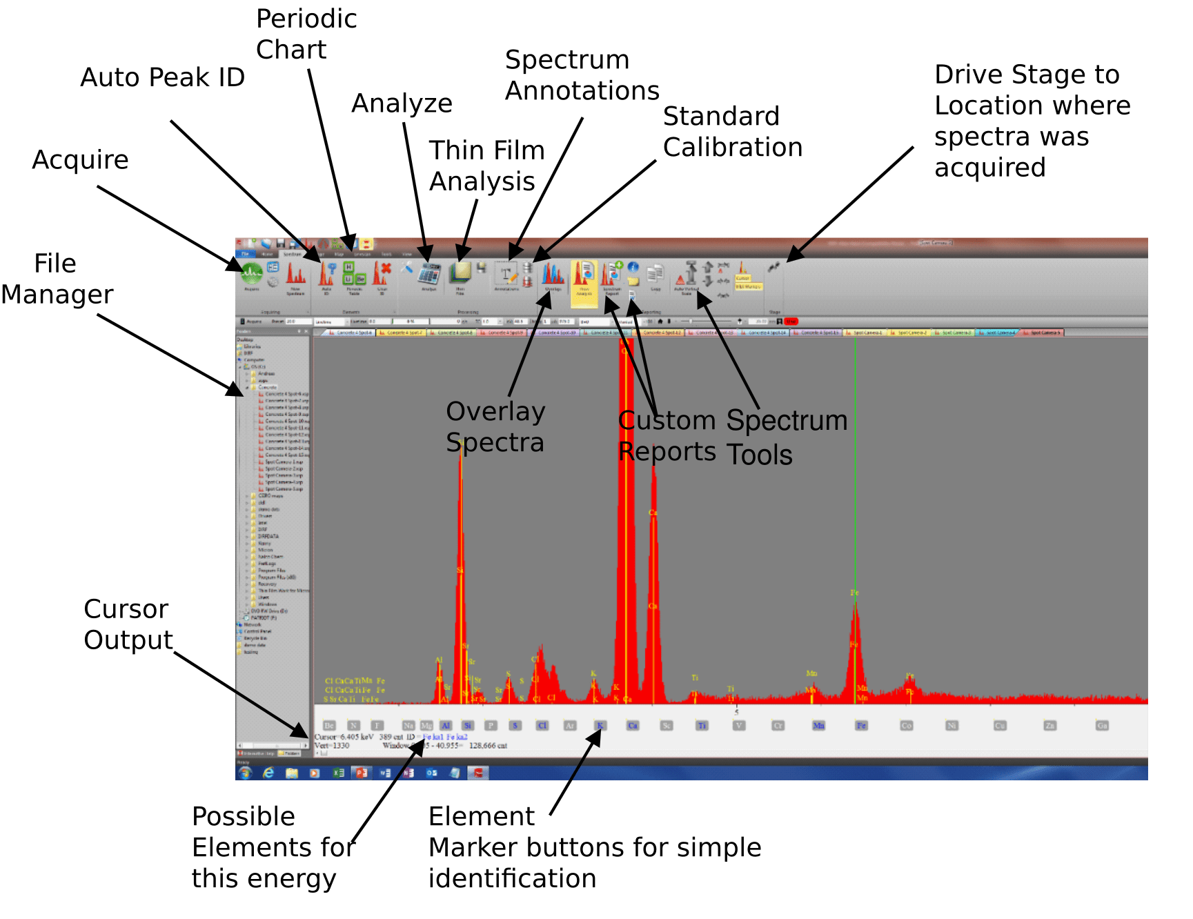
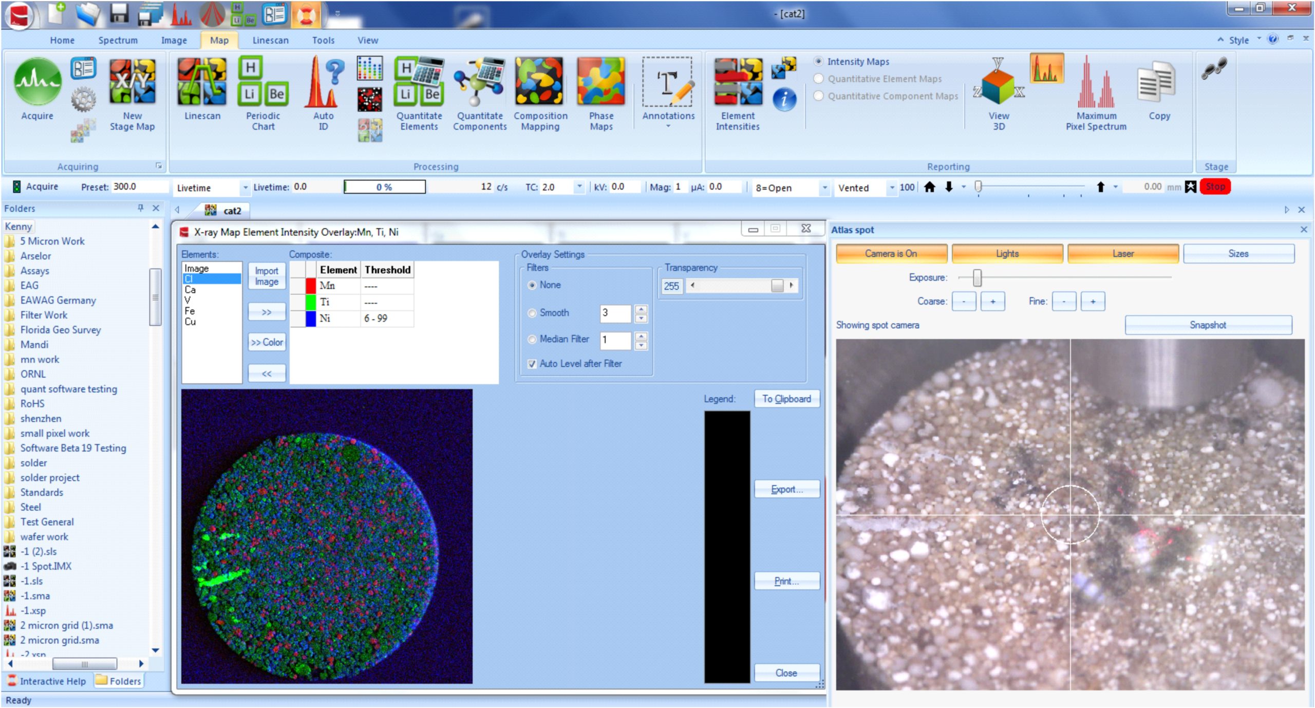
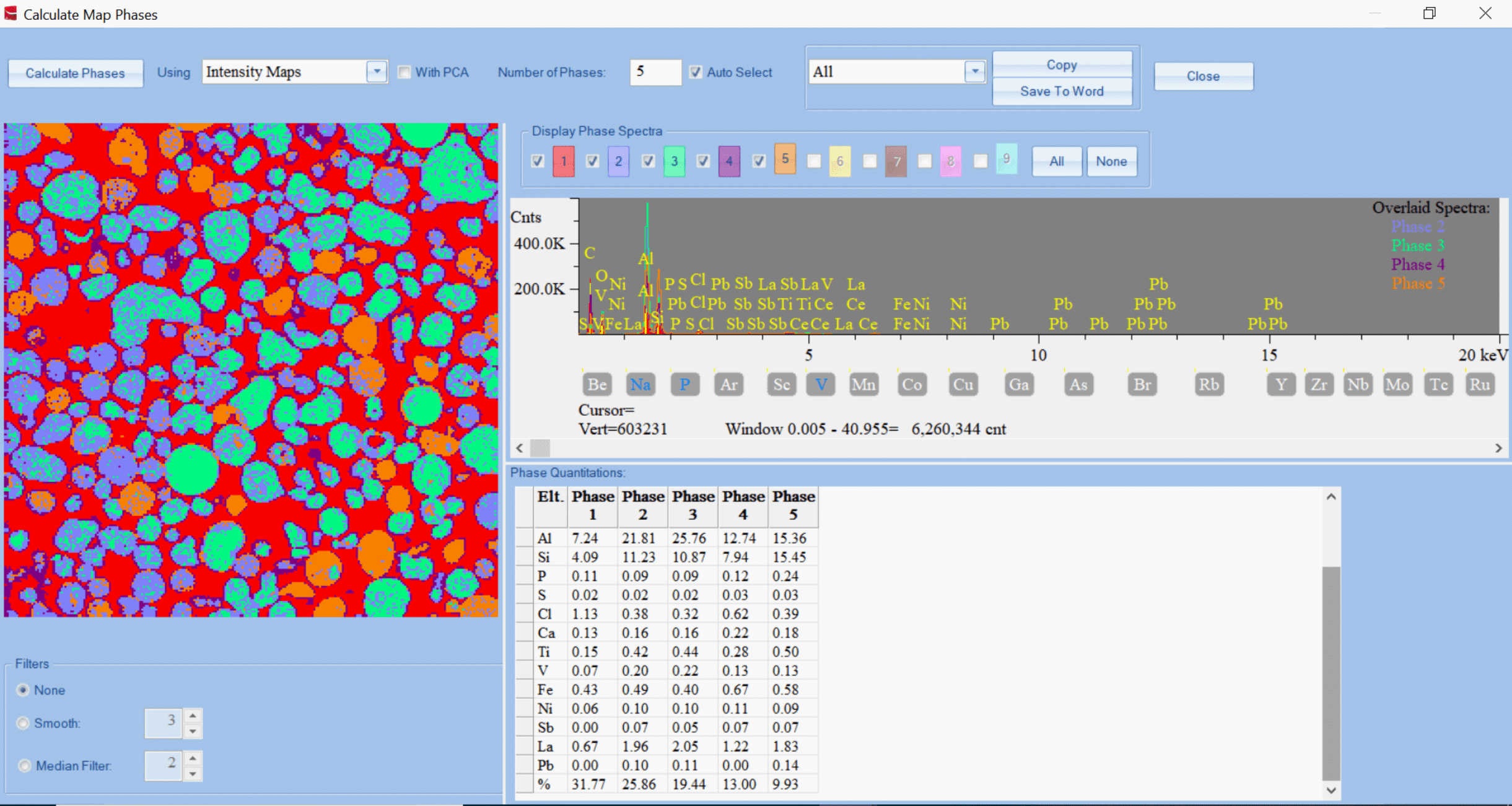
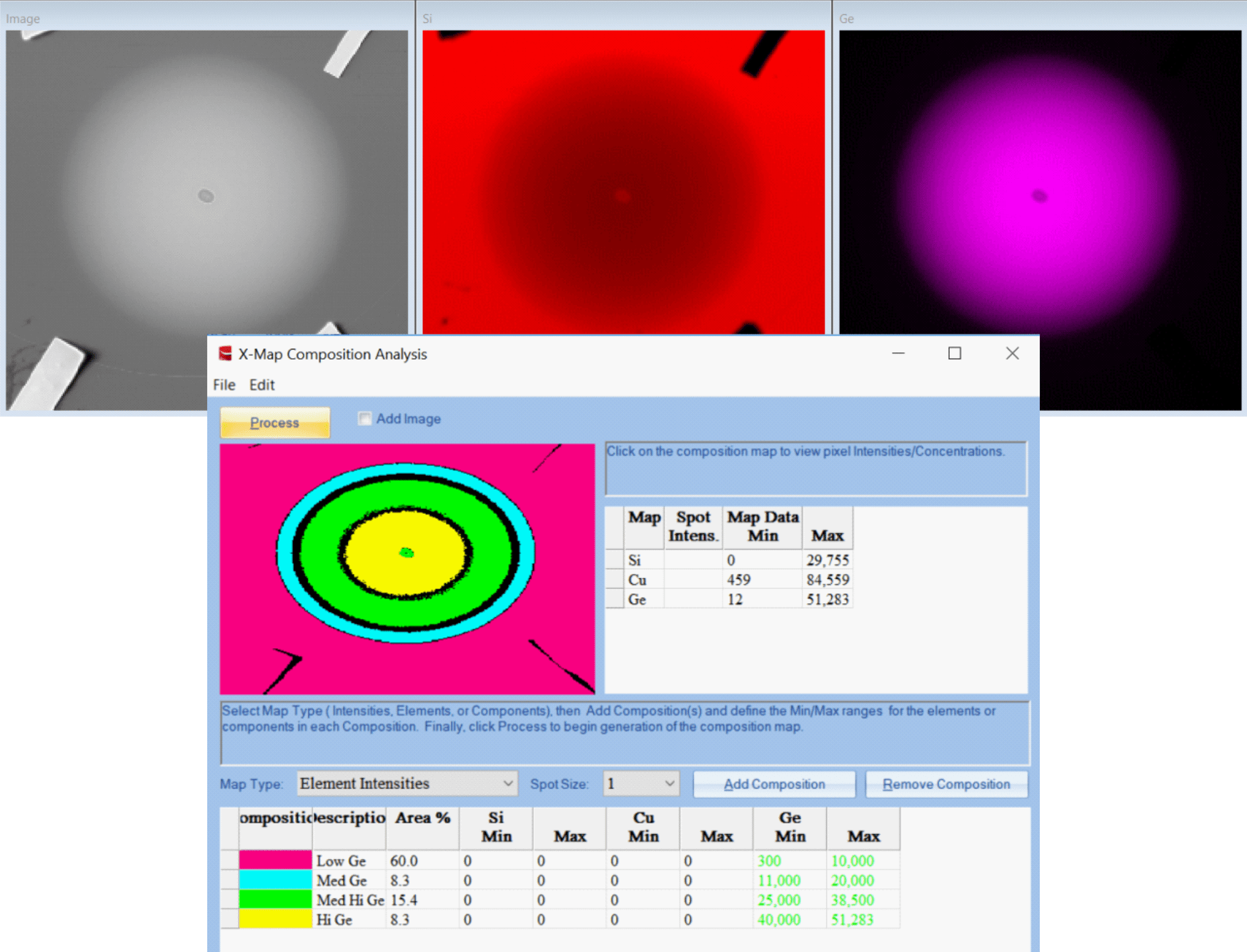
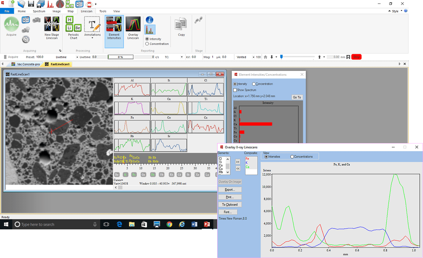
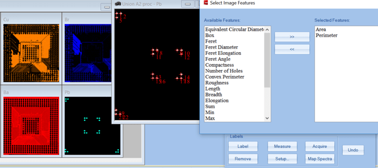
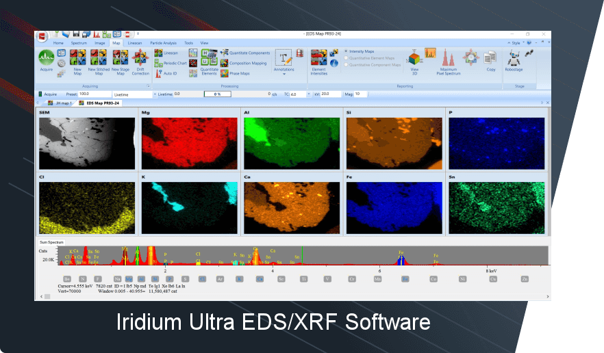
ATLAS’ Iridium Ultra software platform, developed with SEM/EDS elemental mapping and analytical functionality, is unsurpassed in its ability to provide elemental and phase mapping, line scans, critical dimensions (CD), as well as qualitative and quantitative elemental analyses of solids, liquids, particles, powders, and thin films. The functional, flexible, and feature-rich software suite guarantees unprecedented productivity. ATLAS M is the micro-XRF (μXRF) elemental analyzer that leads with innovation.

download a brochure

Made in USAMicro X-ray fluorescence (µXRF, µEDXRF, micro-XRF, microEDXRF) spectroscopy is an elemental analysis technique that relies on the same principles as X-ray fluorescence (XRF) spectrometry. The difference is that micro x-ray fluorescence (microEDXRF) spectrometry has a spatial resolution with a diameter many orders of magnitude smaller than conventional XRF, WDXRF or EDXRF spectrometers. Practically, microEDXRF spectrometers with high-precision scanning XYZ-stages  — like the ATLAS series —  function as a type of  XRF hyperspectral imaging microscope, where each pixel (in a map or image) contains information from 4 – 40 keV in the electromagnetic spectrum.

While a smaller excitation spot can be achieved by restricting X-ray beam using a pinhole aperture, this method blocks much of the X-ray flux which has an adverse effect on the sensitivity of trace elemental analysis. Modern polycapillary focusing X-ray optics are able to create small focal spots of just a few micrometers in diameter. By using such X-ray optics, the IXRF Systems’ ATLAS series of imaging spectrometers provide a tiny focal spot (down to  5 μm, depending on desired configuration) that is much more intense and allows for enhanced trace element analysis and the creation of hyperspectral images of a sample. Micro X-ray fluorescence (μXRF) spectometry is commonly employed in many applications, such as: botany, cement, forensics, small feature evaluations, elemental mapping, mineralogy, metals & alloys, electronics, multi-layered coating analysis, micro-contamination detection, film and plating thickness, biology and environment.*

Atlas Logo

ATLAS microEDXRF elemental maps of K, Ca, Se and sum of X-rays image of a hydrated youngest fully opened leaflet of
Neptunia amplexicaulis (CLICK to ENLARGE)

The 5 micron advantage

ATLAS M is the bench-top micro XRF tool of choice for sample characterization using micro X-ray fluorescence (micro-XRF) hyperspectral imaging microscopy for information on composition (phase) and elemental distribution. With the smallest X-ray spot in the industry at 5 μm, this unique XRF microscope is optimized for analysis speed without compromising accuracy. The instrument can measure a wide range of sample types, whether small or large, even or irregularly shaped. Equipped with a large high-speed stage, it supports 2D analysis of virtually any kind of sample: solids, liquids, powders, thin-films and particles. Its large vacuum chamber delivers superior light element (low-Z) sensitivity.

5um vs 10um spot size

When it comes to XRF microscopic imaging (mapping), smaller is always better. Above is a TEM grid. The image on the left was captured using the ATLAS M's 5 μm X-ray spot. The inferior image on the right was taken with a 10 micron X-ray spot.

ATLAS geometry

ATLAS w/ 5 µm round spot

conventional uEDXRF

Conventional w/ 25 µm oval spot

Superior geometry

  • Perpendicular micro XRF geometry allows for circular excitation down to 5 μm for highest resolution.
  • Beam is normal to the surface for most accurate hyperspectral imaging as beam is NOT an ellipse
  • Competitor’s inferior angled geometry only allows smallest spot to be 25 microns due to the ellipse.

Unmatched speed

  • Mix and match up to 4 Silicon Drift Detectors (SDD)
    • For the largest possible solid angle collection efficiency
  • Up to 600 mm2 active area
    • Available resolutions: ≤130-145 eV resolution
  • Highest count rate with the smallest micro-XRF spot for fast high-res images
Optical kernel

Overview automation

overview automation

Overview video camera mode:

  • Automated spectral spot analysis
  • Automated micro XRF mapping
  • Automated linescans
  • Large chamber view for large samples

Spot automation

spot automation

Video microscope mode:

  • 10 -200X magnification with auto zoom
  • Auto spectral  spot analysis
  • Automated micro XRF mapping
  • Automated linescans

Intuitive software

Beginner users will find the software simple to navigate in a comprehensive manner. As they advance, more powerful tools are easily accessible with no additional cost. They are all included not added on as options:

  • Custom report generation
  • Micro XRF phase analysis
  • Particle analysis via micro XRF
  • Morphology
  • And ASTM testing methods
menu 1
menu 2
menu 3
Liquids and powders

Sample types and conditions

  • Air, vacuum or helium atmosphere
  • Vacuum ready in under one minute
  • Allows, solids, liquids, powders, particles and multi-layer thin films

Made in United States

  • Designed in the USA
  • Manufactured in Austin, Texas
  • Software is written in-house in Austin
Made in U.S.A.

Excitation

  • 50 kV / 50 W / 1 mA Rh target (others available) X-ray tube
  • Polycapillary focusing optic
  • Filter wheel with up to 7 filters (plus open position) before the focusing optic
  • Available primary X-ray spot sizes: 5 , 10, 20 or 40 μm
  • Optional second X-ray tube, with a choice of anodes, is available with spot sizes of 200, 500 or 1000 μm
SDD detectors for SEM
Optical kernel

Detection

  • Mix and match up to 4 Silicon Drift Detectors (SDD)
    • For increased precision and/or reduced acquisition times
  • 50 mm2 to 150 mm2 active area
    • Highest resolution to highest counting rate
  • Available resolutions: ≤130-145 eV resolution
  • Peltier cooling
Quad detectors

High precision stages

  • Motorized XY, Z optional
  • Speeds up to 300mm/s
    • Map acquisitions at ≤ 1ms/pixel
  • Accuracy < 1µm
  • Custom adapters available

Chamber and geometry

  • Chamber size: 508 x 457 x 254 mm (20 x 18 x 10 inches)
  • Top-down perpendicular geometry from tube to sample
  • Mapping area: 220 x 200 mm under automatic control
  • Sample view: 3 sample positioning and analysis cameras
    • Samples may be positioned manually with the door open
Atlas M

Iridium Ultra for Windows® 10

  • Energy dispersive X-ray fluorescence (microEDXRF) spectroscopic software
    • Fundamental Parameters (FP) for solids, liquids, powders and particles
    • Thin film FP for up to 8 layers including an infinite base or substrate
    • Automatic treatment for sum/escape peaks and full deconvolution
    • Up to 8 acquisition conditions per analysis
  • Hyperspectral EDXRF mapping and imaging, up to 4096 x 4096 pixels
    • Every pixel is a full EDXRF spectrum
    • Principal component analysis (PCA) for phase mapping
  • Materials classification database
Iridium Ultra software

Acquisition and quantitation

  • One-click acquisition and automatic peak identification
  • Customizable identification, labeling, processing, and quantification
  • Scrolling periodic chart
  • Drag and drop overlay
  • Automatic overlap correction, sum/escape peak removal, background correction, and linear/non-linear deconvolution
  • Fundamental Parameters (FP) and Quantitative Match
  • Material classification database

Imaging and analysis

  • Multi-Point automated analysis directly from image
  • Morphological processing for rapid feature size measurements
  • Image stitching and montage
  • Segmentation and feature segregation
  • Particle analysis package
    • Including border removal, sorting and exclusion
    • Classification by composition

Mapping and linescans

  • Simultaneous acquisition of 35 elements
  • Stored spectral data for every pixel
  • Live spectrum display during acquisition
  • Single or multiple map acquisition from image
    • Overview or spot camera
  • Map stitching and montage
  • Extract spectra from map: point, area, freehand
  • Create linescan from map
  • Mouse-over view intensities and concentrations
  • Phase Analysis
  • Multi-compositional map display
    • Of element and compound ranges
  • Overlay linescans on image

Specialty and automation

  • Multilayer thin film and coatings analysis up to 8 layers
  • Serpentine continuous mapping (dual directional mapping)
  • ASTM E2926-13 Glass Analysis
  • Track, store, and recall all stage locations and images

Imaging / mapping flow

  • Create multiple X-ray maps on any region on the sample
  • Define map parameters directly from video image
  • Combine pixels to create analysis regions
    • Regions are summed to create a composite spectrum
  • Automatically identify elemental peaks
  • Apply analytical quantification method
  • Analytical results are displayed as a graphic

Top menu navigation

  • Beginner users find the software simple to navigate
  • Advanced users find that powerful tools are easily accessible
  • All software features are included standard
  • Upgrades are free for life, so you are always up to date
  • Custom report generation for completeness
  • Exhaustive toolset comes from scanning electron microscopy

Spectral display features

  • One click operation for acquisition, automatic peak identification, and quantification
  • Collection of x-ray spectra into 25 individual windows
  • Point and click cursor displays energy, counts, and possible elements present
  • Customizable automatic element identification and labeling of peaks
  • Scrolling markers from element chart on spectra
  • Complete annotation tools for spectra; customize text, lines, and more

Alignment laser / operation

  • Comprehensive software design
  • Laser alignment focusing
    • As shown in the video image
  • Large high magnification video viewing
  • Easy to operate joystick
  • Sub-micron X-Y-Z stage
  • Alignment laser visible on concrete sample

Automatic phase analysis

  • Phase analysis by Principle Component Analysis (PCA)
  • PCA is used in exploratory data analysis, an approach to analyzing data sets to summarize their main characteristics
  • PCA can be done on intensity or concentration based maps
  • Phases are defined and percent (%) of field of view of each phase is defined
  • In a PCA map, phases are marked by a defined color

Imaging composition

  • User defined compositions define the image
  • Maps can be defined by intensities or concentrations
  • Maps can be elements, compounds, components, materials, etc.
  • Example top series starts with a composite grey scale of a sample
    • Key: red is high Si areas and purple is high Ge
  • Inset image show a more complicated composition analysis map

Click Image to Enlarge

Line profile analysis (linescan)

  • Relative elemental concentration or intensity along a line
  • Multiple charts display the “tiled” form of the data
    • Relative change of each element is viewed separately
  • Linescans may also be displayed “stacked” for comparison
    • Inset example shows an overlay of a long 300 mm linescan
  • Larger image is  a 5 micron scan at ppm levels

Morphology

  • Surface morphology is a evaluation of the shape of a surface
  • Particles, features, inclusions are elementally identified
    • And automatically counted/measured by feature type
  • Additional data on each feature may be easily collected
  • As shown, an extensive set of image features is available

ATLAS M features

  • Benchtop / tabletop form factor
  • Spot size down to 5 microns with anti-halo optic
  • SDD detectors w/ active area up to 150 mm2
  • Large chamber volume
  • 50 kV / 50 W polycapillary optic X-ray source
  • Multi-point/multi-area automation & mapping
  • Air, vacuum, helium for solids, liquids, and powders
  • Iridium Ultra software running on Windows™ 10 OS

Specifications

Specifications

Elemental range:

Sodium (Na) through uranium (U)

Sample types:

Solids, liquids, particles, powders and thin films

Sample chamber size:

508 x 457 x 254 mm (20 x 18 x 10 inches)

Analysis atmosphere:

Air, vacuum or He(g) purge

Primary X-ray source:

50 W max power, 50 kV @ 1 mA

Optional secondary X-ray source:

4-12 W max power,  40-60 kV @ 0.4-1 mA

X-ray source optics:

Polycapillary or aperture collimation

X-ray source anode:

Rhodium (others optionally available)

X-ray source spot size (primary):

5 μm standard (optional: 10, 20 or 40 μm)

X-ray source filters:

Up to 7 plus an open position

Primary X-ray source geometry:

Top-down beam (perpendicular to sample stage)

Detector(s):

1 standard, optionally up to a maximum of 4

Detector types:

Silicon drift detector (SDD) standard (PIN-diode is optionally available)

Detector active area:

50 to 150 mm2, up to 600 mm2 w/ 4 detectors

Sample stage type:

Motorized X,Y and Z (optional)

Sample stage travel:

320(W) x 320(D) x 210(H) mm

Mapping travel:

220(X) x 200(Y) mm

Mapping scan speed:

1-3 ms/pixel

Stage XY speed:

Up to 300 mm/s

Sample view:

3 cameras for sample positioning and analysis

Operating system:

SFF PC w/ Microsoft® Windows™ 10 OS

Analysis and control software:

Iridium Ultra: provides complete control of parameters, filters, cameras, optical microscopes, sample illumination and positioning, and measurement media

Quality and safety:

CE marked, RoHS, radiation < 0.5 μSv/h

Dimensions:

951(L) x 556(W) x 564(H) mm (38 x 22 x 22 inches)

Power:

100-240 V, 1 phase, 50/60 Hz

Periodic table

  • Quantify elements from sodium (Na) through uranium (U)
  • In any sample type: solids, liquids, powders, particles and thin films
  • From low parts-per-million (PPM) to 100 wt.%
  • Hyperspectral microscopic imaging
    • where every pixel is a complete spectra
  • Mapping, linescans, multi-point and single point quantification
Periodic Table of the Elements
ASTM E-2926-13

Forensic glass analysis

  • Full compliance with ASTM E-2926-13
  • Automation software option for analyzing glass for forensic court cases
  • Software Features:
    • Simple “Wizard” software approach for standard calibrations.
    • Automatically calculates difficult ratios and statistics required
    • Automatically creates Excel spread sheets as required reporting structure for court cases

Life sciences

  • Hyperspectral XRF microscopy
  • From anatomy to biology to botany and beyond
  • 100% Nondestructive
  • Unlike a SEM, there is no coating or sample prep
  • Works with non-conductive samples
  • Automatically produce quantitative analysis for each pixel
paint chip forensics

Forensics for paint chips

  • Very powerful forensic  tool capable of single or multi-spot analysis
  • Hyperspectral XRF microscopic elemental quantitative imaging
    • To identify distribution of elements within a sample
    • Paint chip and paint layer analysis is a common forensic application
  • Differentiate closely related samples
    • By the coating, paint, or base coat in any combination

Circuit board inspection

  • Fast X-ray mapping for electronics’ inspections
  • A complete X-ray Spectrum for each pixel in the map
  • Measure thin gold and palladium coatings on PCBs
  • Measure coating thickness of Cu, Ni, etc.
  • Measure solder composition
  • RoHS / WEEE compliance
Circuit Boards
Lead Frame

Lead frame imaging

  • Measurements on very small flat components and structures such as conducting paths, contacts or lead frames
  • Measurements of typical multi-coating systems on lead frames,e.g., AuAg/Pd/Ni/CuFe or Au/Pd/Ni/CuFe in the nanometer range
  • Determination of the phosphorous content in NiP coatings
  • Measurements of functional coatings in the electronics and semiconductor industries
  • Determination of complex multi-coating systems

Wafer metrology

  • Sn/Ag Bump/Pillar measurements
  • Light elements
  • Metal film stack composition such as CIGS
  • Cu CMP control at BEOL
  • Multi-stack structures
  • Sputtering targets
  • Thermal barrier coating
  • Thickness and composition control
Semi Software
Pharmaceutical

Pharmaceuticals

  • Trace XRF spectrometry mapping at 5 microns
  • Trace analysis of metal impurities and inclusions
  • Non-destructive elemental analysis
  • Quality control / quality assurance
  • Particle analysis
  • Distribution and/or phase analysis

Soils and drilling cores

  • Quick phase maps using Principal Components Analysis (PCA)
  • Quickly map samples for trace hazardous elements within automatically in minutes
  • No sample preparation
  • Analysis in atmosphere, under helium or in a vacuum
  • Mineral identification
  • Phase boundaries
Soils
steel centerline segregation
Mn segregation

Metals & alloys

  • Advanced continuously cast high strength low alloy steels are often subject to elemental segregation along the billet or slab centerline during casting and cooling
  • With mapping, micro-spot energy dispersive X-ray fluorescence (microEDXRF) spectroscopy, it is possible to rapidly scan centerline areas and quantitatively monitor elemental inhomogeneity
  • While many key elements co-segregate in continuously cast high strength steels, of particular interest is manganese (Mn) which is the primary hardening agent that can easily be measured in an air environment
  • Other segregating elements of interest include: Cr, Ni, Mo, S, P, Al and Si

Geology

  • Small spot, microEDXRF expands the abilities of a geologist. Micro-XRF is ideally suited for the analysis of inorganic species, and offers excellent sensitivity to trace elements and phases
  • Point analysis allows fast identification of mineral phases, even when analyzing individual grains from crushed rock, or microscopic features in a section
  • XRF hyperspectral imaging provides detailed element images which highlight the distribution of mineral phases, illustrating the general rock structure
• Geological thin slices
• Mineral identification
• Phase boundaries
• Meteorites
• Volcanic material
• Sediment cores
• Mining test cores
• Mining exploration
• Gemstones
Geology mineral phases
cement aggregate

Cement & aggregate

  • Elemental mapping of concrete and cements may be performed with ATLAS providing the analyst with the opportunity to visually and chemically inspect the physical sample
  • XRF is the established technique to control the quality and conformity of the final cement product
  • Phase mapping of concrete cores provides quantitative aggregate distribution data

RoHS / WEEE

  • With stage mapping, large samples can be quickly mapped for identification of prohibited materials
  • It is not necessary y to know what elements are present before collecting a map
  • Elements can be added as the spectrum grows and peaks become evident
  • ATLAS X offers the largest sample chamber in the industry
Archaeometry Louvre Museum

Archaeometry

  • Sensitive and valuable archaeological objects can be easily and reliably analyzed with the ATLAS Micro-XRF spectrometer
  • The microEDXRF (μXRF) technique permits a fast non-destructive analysis of objects, especially on small sample areas
  • ATLAS X offers the largest vacuum chamber in the industry to allow low-Z elements of large objects to be analyzed

CIGS solar cells

  • Analysis of thin film photovoltaic cells is commonly performed with Micro-XRF
  • With ATLAS, it is possible to measure structures under vacuum for superior results
  • For in-line control during the production process as well as for final testing
  • Quantification for layer thicknesses are in very good agreement with WDXRF results
CIGS solar cell

Reference documents

      • “Company Index: A Guide to Companies.” Microscopy Today 21, no. S1 (March 2013): 50–55. https://doi.org/10.1017/S1551929513000357.
      • Do, Christina, Farida Abubakari, Amelia Corzo Remigio, Gillian K. Brown, Lachlan W. Casey, Valérie Burtet-Sarramegna, Vidiro Gei, Peter D. Erskine, and Antony van der Ent. “A Preliminary Survey of Nickel, Manganese and Zinc (Hyper)Accumulation in the Flora of Papua New Guinea from Herbarium X-Ray Fluorescence Scanning.” Chemoecology 30, no. 1 (February 1, 2020): 1–13. https://doi.org/10.1007/s00049-019-00293-1.
      • Ent, Antony van der, Peter M. Kopittke, David J. Paterson, Lachlan W. Casey, and Philip Nti Nkrumah. “Distribution of Aluminium in Hydrated Leaves of Tea ( Camellia Sinensis ) Using Synchrotron- and Laboratory-Based X-Ray Fluorescence Microscopy.” Metallomics 12, no. 7 (2020): 1062–69. https://doi.org/10.1039/C9MT00300B.
      • Harvey, Maggie-Anne, Erskine, Peter D., Harris, Hugh H., Brown, Gillian K., Pilon-Smits, Elizabeth A. H., Casey, Lachlan W., Echevarria, Guillaume and van der Ent, Antony (2020). Distribution and chemical form of selenium in Neptunia amplexicaulis from Central Queensland, Australia. Metallomics 12 (4) 514-527. https://doi.org/10.1039/c9mt00244h.
      • Van der Ent, Antony, Casey, Lachlan W., Blamey, F. Pax C. and Kopittke, Peter M. (2020). Time-resolved laboratory µ-XRF reveals silicon distribution in relation to manganese toxicity in soybean and sunflower. Annals of Botany. https://doi.org/10.1093/aob/mcaa081.
      • Huang, Xitong, Yong Li, Ke Chen, Haiyan Chen, Fei Wang, Xiaomin Han, Beihai Zhou, Huilun Chen, and Rongfang Yuan. “NOM Mitigates the Phytotoxicity of AgNPs by Regulating Rice Physiology, Root Cell Wall Components and Root Morphology.” Environmental Pollution 260 (May 2020): 113942. https://doi.org/10.1016/j.envpol.2020.113942.
      • Jones, Michael W. M., Peter M. Kopittke, Lachlan Casey, Juliane Reinhardt, F. Pax C. Blamey, and Antony van der Ent. “Assessing Radiation Dose Limits for X-Ray Fluorescence Microscopy Analysis of Plant Specimens.” Annals of Botany 125, no. 4 (March 29, 2020): 599–610. https://doi.org/10.1093/aob/mcz195.
      • Le Pape, Y. “Neutron-Irradiation-Induced Damage Assessment in Concrete Using Combined Phase Characterization and Nonlinear Fast Fourier Transform Simulation.” In Proceedings of the 10th International Conference on Fracture Mechanics of Concrete and Concrete Structures. IA-FraMCoS, 2019. https://doi.org/10.21012/FC10.232765.
      • Li, Y., Y. Le Pape, E. Tajuelo Rodriguez, C.E. Torrence, J.D. Arregui Mena, T.M. Rosseel, and M. Sircar. “Microstructural Characterization and Assessment of Mechanical Properties of Concrete Based on Combined Elemental Analysis Techniques and Fast-Fourier Transform-Based Simulations.” Construction and Building Materials 257 (October 2020): 119500. https://doi.org/10.1016/j.conbuildmat.2020.119500.
      • Pearson, Charlotte, Matthew Salzer, Lukas Wacker, Peter Brewer, Adam Sookdeo, and Peter Kuniholm. “Securing Timelines in the Ancient Mediterranean Using Multiproxy Annual Tree-Ring Data.” Proceedings of the National Academy of Sciences 117, no. 15 (April 14, 2020): 8410–15. https://doi.org/10.1073/pnas.1917445117.
      • Ye, Hui, Changzhi Wu, Matthew J. Brzozowski, Tao Yang, Xiangping Zha, Shugao Zhao, Bingfei Gao, and Weiqiang Li. “Calibrating Equilibrium Fe Isotope Fractionation Factors between Magnetite, Garnet, Amphibole, and Biotite.” Geochimica et Cosmochimica Acta 271 (February 2020): 78–95. https://doi.org/10.1016/j.gca.2019.12.014.
      • Zhang, Mingyuan, Jianxiang Wang, and Li-Hua Shao. “Ultrahigh Flexoelectricity of 3D Interconnected Porous PDMS.” ArXiv:2009.03847 [Physics], September 27, 2020. http://arxiv.org/abs/2009.03847.
      • Ziejewska, Celina, Joanna Marczyk, Aneta Szewczyk-Nykiel, Marek Nykiel, and Marek Hebda. “Influence of Size and Volume Share of WC Particles on the Properties of Sintered Metal Matrix Composites.” Advanced Powder Technology 30, no. 4 (April 1, 2019): 835–42. https://doi.org/10.1016/j.apt.2019.01.013.

Search terms

  • XRF
  • X-ray fluorescence
  • X-ray fluorescence spectroscopy
  • X-ray fluorescence spectrometry
  • energy dispersive X-ray fluorescence
  • energy dispersive X-ray fluorescence spectroscopy
  • energy dispersive X-ray fluorescence spectrometry
  • micro X-ray fluorescence
  • micro X-ray fluorescence spectroscopy
  • micro X-ray fluorescence spectrometry
  • micro energy dispersive X-ray fluorescence
  • micro energy dispersive X-ray fluorescence spectroscopy
  • micro energy dispersive X-ray fluorescence spectrometry
  • μXRF
  • mXRF
  • μEDXRF
  • mEDXRF
  • microXRF
  • microEDXRF
  • micro-XRF
  • m-XRF
  • micro-EDXRF
  • m-EDXRF
  • small spot XRF
  • small-spot XRF
  • small spot EDXRF
  • small-spot EDXRF

Suggested Products

ATLAS SEMISEM-XRF Systems
Interested in what we do?

CONTACT US

  • Hi, my name is
  • and I am interested
  • in the
  • Please contact me at
  • or call me at
  • This field is for validation purposes and should be left unchanged.