microXRF X-ray sources for Scanning Electron Microscopes (SEM): addition of an polycapillary X-ray tube and Iridium Ultra software will transform your SEM’s quantitative analytical capabilities. Higher peak to background ratios enable greater elemental sensitivity for higher Z elements: sensitivity exceeding e–-beam excitation by a factor of 10-1000X. Exceptional beam stability, together with a modern SDD X-ray detector, afford higher precision with ppm-level sensitivity. Non-conductive materials may be analyzed without any special preparation or coating. We integrate with your SEM to deliver full spectrum analysis using excitation from both the e–-beam and our X-ray source.
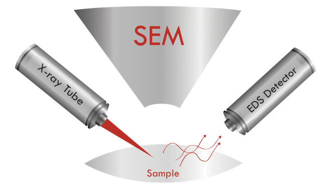
SEM-XRF : Integrated e⁻-Beam / X-ray XRF Elemental Analysis
X-ray Sources for Electron Microscopy (SEM)
What is SEM-XRF?
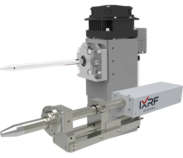
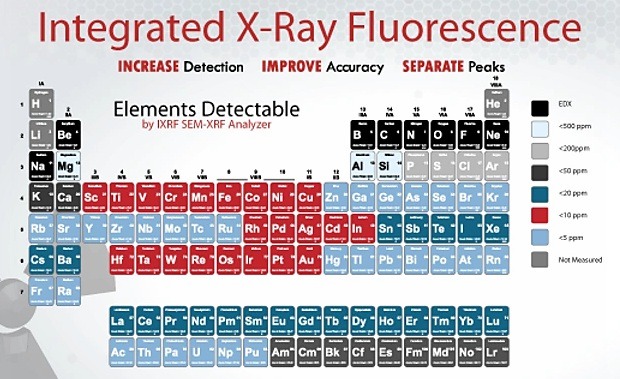
IXRF’s Xb SEM micro-spot X-ray source adds the capabilities of a complete micro X-ray fluorescence (microXRF) spectrometer to a scanning electron microscope (SEM). Xb SEM fits on an unused or open high-angle port of almost any SEM. Total non-destructive, μXRF users benefit from both superior trace element sensitivity and broader elemental coverage (Na through U using K- and L-lines) .
Relative sensitivities of K-lines at 30 kV excitation.
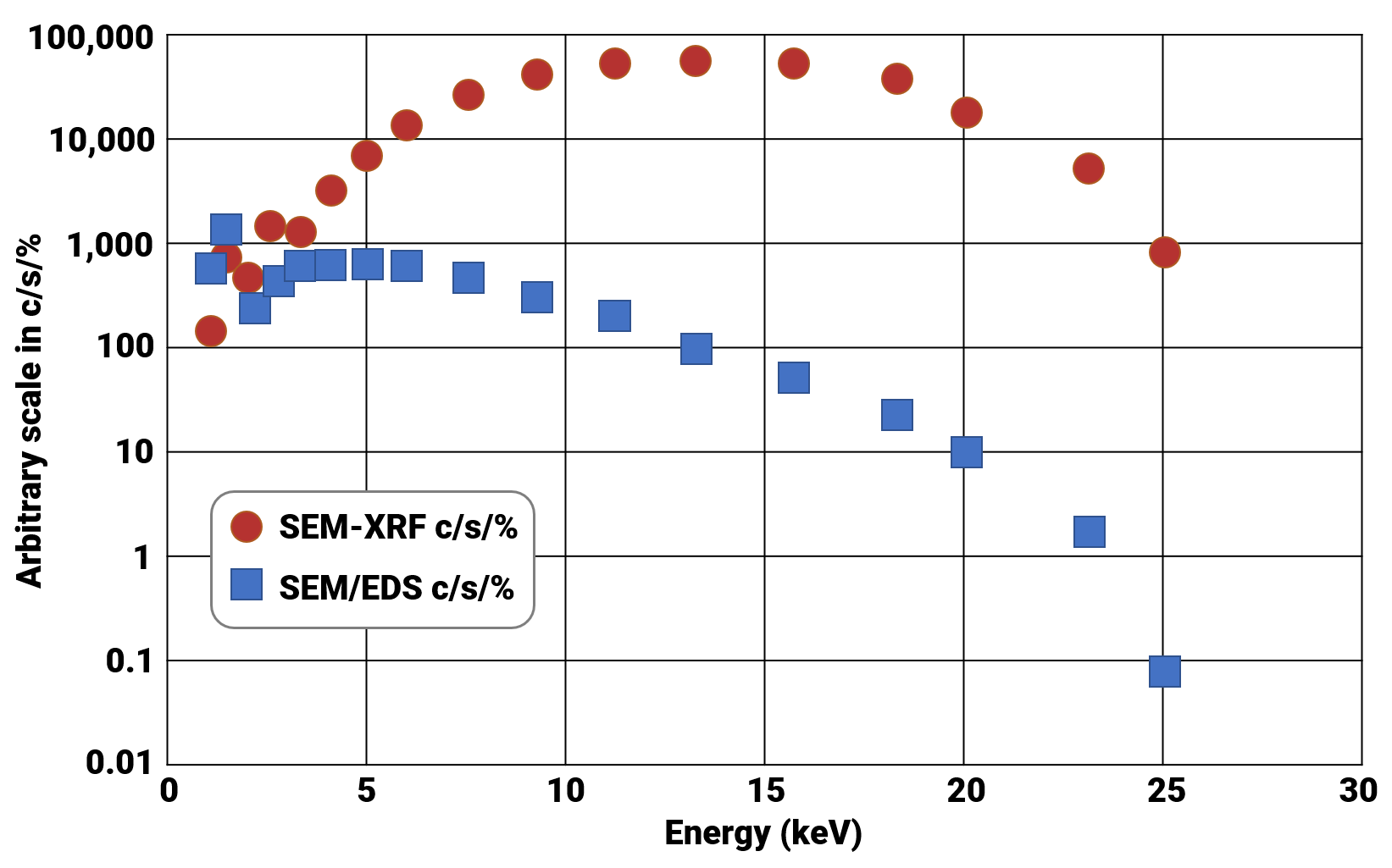
At left is shown a plot of a theoretical silicon sample containing trace amounts of Na-Sn. At 0-2 keV, e-beam (SEM/EDS) is clearly more efficient. Above about 2 keV, X-ray photon excitation (SEM-XRF) becomes orders of magnitude more efficient. This allows for quantification of more elements at lower concentrations than is possible with SEM/EDS.
Advanced microXRF System for SEM
Distribution analysis stores complete spectra for every map point for on- and off-line analysis. Samples can be analyzed with micro-spot X-ray beam and e⁻-beam simultaneously without position change. Both excitation methods are integrated in our analytical software suite. No interference with normal SEM operation, the X-ray source can stay in its measurement position permanently. microXRF is completely non-destructive and does not require the sample to be coated. Use your existing EDS detector system; we support most all microscopes.
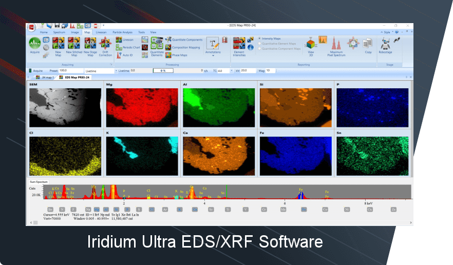
Elemental Analysis with a microXRF Spectrometer
- • Analytical results compare to those of standalone μXRF systems
- • State-of-the-art analytical software: Iridium Ultra
- – Decades of continuous development & innovation
- • Selectable primary X-ray filters
- – To suppress Bremßtrahlung and diffraction peaks
- – For lower detection limits, down to PPM levels for most elements
- • Uses your scanning electron microscope’s motorized stage
- • Allows sample tilt to produce minimum spot sizes
- • No special cooling is required, our sources are air cooled
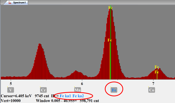
Chemical Composition by Rayleigh to Compton Ratio Method
 Another advantage of having micro-XRF in a scanning electron microscope (SEM) is the ability to employ the characteristic lines from the anode material (typically Ag, Cu, Mo, Rh or W) of a X-ray tube to non-destructivity determine the average atomic number of any phase or artifact. The high specificity of elastic (Rayleigh), as well as inelastic (Compton), X-ray scattering to the mean atomic number of a specimen has long been recognized.1 Micro-spot X-ray fluorescence (micro-XRF) may thus be exploited to non-destructively gain more information on chemical composition. In practice, the Rayleigh/Compton intensity ratio from XRF spectra may be calibrated, with standard reference materials, relative to mean atomic number. This sort of calibration curve can reveal valuable information on the elemental composition complementary to that obtained from conventional elemental analysis via XRF-SEM and/or SEM/EDS. Particularly for matrices of lower mean atomic numbers (like plastics), the sensitivity of the approach is so high that it can be easily distinguish between specimens of mean atomic numbers differing from each other by 0.1 Z. Hence, the content of light elements which are “invisible” for XRF, particularly hydrogen, or of heavier impurities/additives in light materials can be calculated “by difference” from the scattering calibration curve.
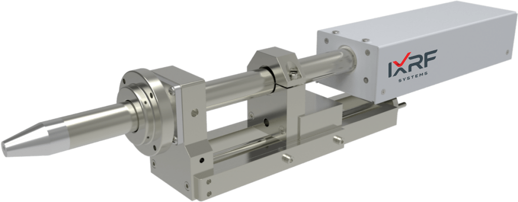
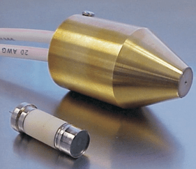
Xb Product Features
IXRF’s Xb custom micro-spot X-ray source is designed exclusively for use on electron microscopes. A compact design with slide mounting allow very close coupling to the sample. Patented polycapillary optics focus X-ray photons down to sample spot size as small as 10µ. Xb is offered in 10µm and 40µm spot sizes. An integrated high-voltage power supply operates up to a maximum power of 50 watts (35-50 kV and 1.0 mA depending on anode material). Close coupling provides XRF analytical results comparable to those from traditional “’benchtop EDXRF” or “mainframe” XRF instruments. An additional benefit is that the Xb X-ray source is designed so that it does not interfere with the normal operation of the electron microscope, including the use of the electron beam on the same sample at the same time so as to simultaneously collect data on all elements.

SEM-XRF Advantage: Quantify Trace Elements
Electron beams (from scanning electron microscopes) produce very high backgrounds, hiding trace elements in a sample. Direct X-ray excitation from a true “X-ray source” don’t have this effect. Using IXRF’s Xb, low ppm levels of elements can be easily identified, quantified … even producing trace level X-ray maps to view elemental distribution of trace elements in your sample. For elements above Na, limits of detection (LOD) can be as low as 10 ppm, depending on element and matrix.
SEM-XRF Advantage: Broad Elemental Coverage
X-ray excitation up to 50 kV, together with a variety of available primary filters, allows for high-sensitivity analysis of first and second row transition metals (using K-lines). Even heavier elements may be similarly analyzed using their L-lines.
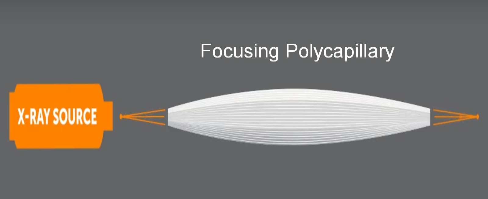
Polycapillary Optics' Advantage
Polycapillary focusing optics collect a large solid angle of X-rays from an X-ray source and focus them to a spot as small as 10 µm. The X-ray flux density obtained is a few orders of magnitude higher than that obtained with a conventional pinhole collimator. The main application of these optics is micro X-ray fluorescence (µXRF) analysis, which has been widely used for thin film and plating analysis, precious metal evaluation, alloy measurement, and monitoring of electric circuit board coatings. Use of polycapillary focusing optics will significantly enhance the detection sensitivity and allow the high performance to be achieved with low-powered X-ray tubes. Micron-sized spatial resolution makes small feature evaluation possible for electronics and precious metal applications. Polycapillary optics offer 100x-10,000x gain with output focal spot sizes as small as 10 µm.
Product Specifications
Xb
ANODE TYPE
Side-window
TARGET MATERIAL
Ag, Cu, Mo, Rh & W
ACCELERATING VOLTAGE
0-50 kV
BEAM CURRENT
Max 1 mA
EXCITATION SPOT SIZE
10, 20, 40 µm
COLLIMATOR SIZE
Patented polycapillary focusing optic
SOURCE FILTERS
Available upon request
COOLING REQUIREMENTS
Air cooled (fan)
CONTROLS / SAFETY
Variable control kV/µA, X-ray on/off buttons, kV/µA display, internal interlocked shutter. Interlocked to SEM, keyed power-on switch, HV-On lamp, warning beacon
ƒX Product Features
IXRF’s new ƒX SEM™ is an affordable, air-cooled custom X-ray source option designed exclusively for use on electron microscopes. With a compact design and slide mounting, very close coupling to the sample is achieved. This unique design delivers “high flux” X-rays to small or large excitation areas on a sample’s surface. The ƒX SEM™ offers excitation spots ranging from 500 µm to 25 mm (ellipse minor side width).
Supported On All SEM Brands
The integrated high-voltage power supply operates up to a maximum power of 10 W (35 kV and 0.1 mA depending on anode material). Close coupling provides X-ray fluorescence (XRF) spectrometry analytical results comparable to those from a traditional benchtop EDXRF operating under a vacuum atmosphere. The ƒX SEM™ is designed so that it does not interfere with the normal operation of the electron microscope, including the use of the electron beam on the same sample, at the same time collecting all elements simultaneously.
Non-destructively Quantify and Map Trace Elements
Electron beams (from scanning electron microscopes) produce very high backgrounds hiding the trace elements in the sample. X-rays, from a true “X-ray source” don’t have this effect. Using the ƒX SEM™ low ppm levels of elements can be easily identified and quantified … even producing trace level X-ray maps to view elemental distribution of trace elements in your sample.
Product Specifications
ƒX
ANODE TYPE
End-window transmission
TARGET MATERIAL
Ag, Mo & W
ACCELERATING VOLTAGE
10-35 kV
BEAM CURRENT
0-100 µA
COLLIMATOR SIZE
200, 500 and 1000 µm (others available)
SOURCE FILTERS
Available upon request
COOLING REQUIREMENTS
Conduction cooled, no fan required
CONTROLS/SAFETY
Variable control kV/µA, X-ray on/off buttons, kV/µA display. Interlocked to SEM, keyed power-on switch, Integrated high-voltage power supply, HV-On lamp, warning beacon
X-ray Source + SEM =
- Sensitivity: Higher peak to background ratios enables greater elemental sensitivity for higher Z elements; sensitivity exceeding SEM/EDS by a factor of 10-1000x.
- Precision: The extreme X-ray beam stability of Xb, coupled with premium SDD X-ray detectors, yields highest possible precision and lowest achievable detection limits.
- Accuracy: Using elemental K-lines (and L-lines of high-Z elements) means less complex deconvolution of various peak overlaps.
- Non-destructive: Analysis of non-conductive materials without coating or e⁻-beam damage.
- Full elemental coverage: Integrated with EDS software for the most accurate low energy-high energy (full spectrum) analysis available (by combining e⁻-beam and X-ray beam excitation).
Fits Your Microscope
X-ray tube additions may be interfaced to almost any brand and model of SEM. High angle (35º) as well as horizontal flange mounts are available for every tube package.
Polycapillary Optics
IXRF’s Xb delivers the addition of focusing capillary optics to enable microspot XRF analysis down to 10 microns. A greatly reduced spot size increases micro-XRF X-ray elemental mapping capabilities and enhances trace elemental and/or thin-film analysis at the micron level.
10 μm Spatial Resolution
This is a picture of a 12 micron Ni grid X-ray map. The grid is imaged with a 10 micron Xb X-ray source demonstrating exceptional spatial resolution.
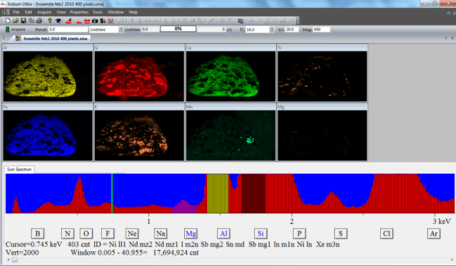
Combined EDS and XRF X-ray mapping bring previously unseen capability to the electron microscopist.
X-ray Tube Automation
Packaged tubes may be operated up to 50kV and come with integral high voltage power supplies. Power supplies are integrated with interlocking vacuum sensors which shut off the x-rays when the SEM chamber is vented. Each unit automatically “ramps” the tubes for increased longevity.
Miniaturization
The chief component of low cost X-ray Fluorescence brought into the electron microscope chamber is the ƒX SEM™ low powered transmission target X-ray tube. The tubes are reduced in size and produce less heat than larger, higher powered tubes. Mo, W and Ag thin film targets deposited on a Be window are available for optimizing varying applications.
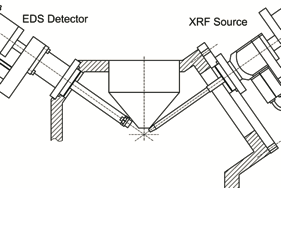
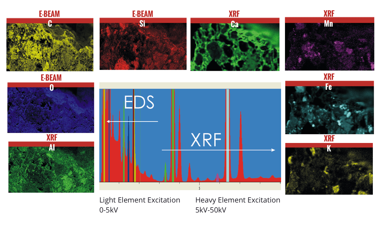
X-ray source & Electron Beam Integrated Acquisition
Electron Beam Excitation
In order to acquire the most comprehensive and accurate full spectrum in seconds, use your EDS system to capture the light elements between 0-3kV; use the iXRF SEM-XRF tool to acquire the heavier, higher energy elements between 3-50kV.
Combined Quantification
In order to acquire the most comprehensive and accurate full spectrum in seconds, use your EDS system to capture the light elements between 0-3kV; use the iXRF SEM-XRF tool to acquire the heavier, higher energy elements between 3-50kV.
X-ray Source Excitation
Acquire your full spectrum using one technique at a time or run in simultaneous mode. Acquire light and heavy elements using two techniques at the same sample location without ever opening the chamber.
Available Methods
- Auto
- ZAF
- FP
- Least Squares
- Match
SEM-XRF Dual Excitation
The IXRF SEM-XRF option, offers the ability to use both the electron beam and Micro-XRF beam simultaneously. With the electron beam at 3-5kV, only the light elements are excited. There is no significant background added to the XRF spectra, allowing all the elements in the sample to be seen.
Applications
XRF provides non-destructive analysis of various sample sizes and sample types including solids, environmental samples, powders and residues. Below are examples of common applications for traditional tabletop (bench top) XRF that are now available inside the SEM:
- Art and Archeological
- Chemical
- Coatings and Thin Film
- Cosmetic
- Educational
- Environmental
- Food Applications
- Forensics
- Metal and Ore
- Mineral and Mineral Products
- Petroleum EDXRF
- Pharmaceutical Applications
- Plastics, Polymers, and Rubber
- Plating and Plating Baths
- Wood Treating
- Concrete Treating
- And Others

Mapping
Trace elemental mapping is possible for nearly all of the above applications. XRF mapping can be performed using either of our products; shown here by this mineral map using the X-Beam.
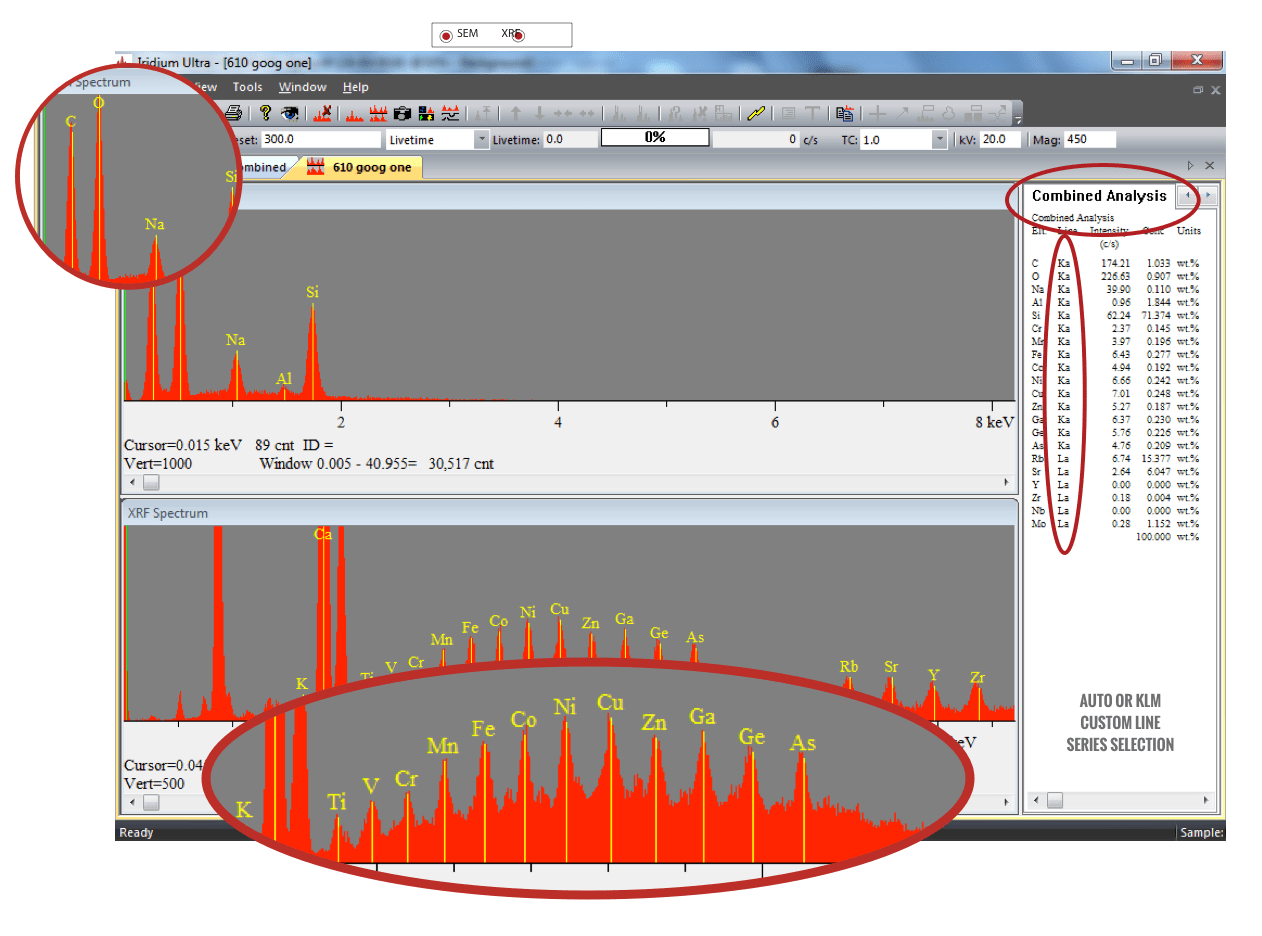
Sensitivity: Glass
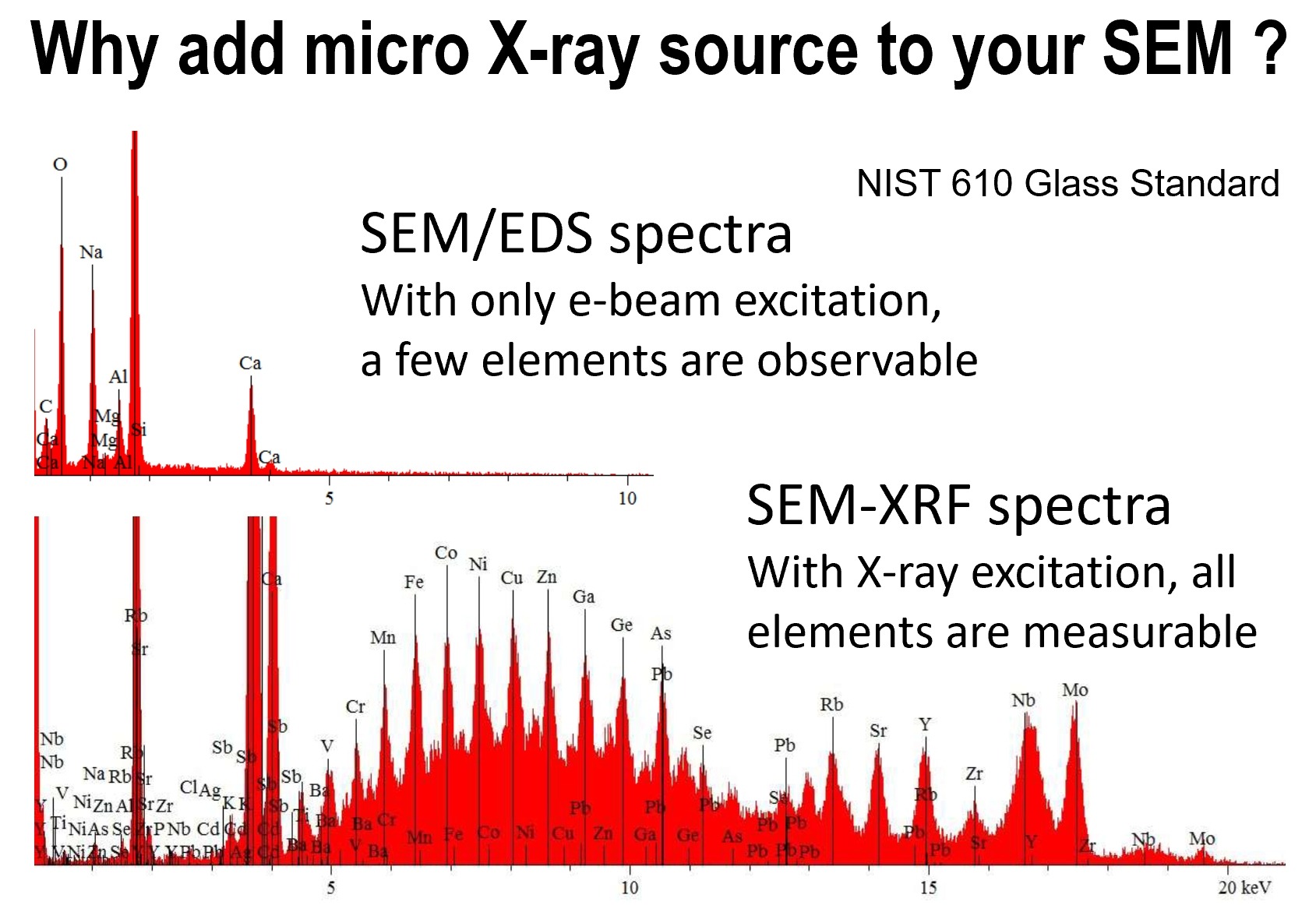
XRF can be used for trace spectral acquisition down to low PPM levels. XRF can be 10-1000 times more sensitive than SEM-EDS analysis, exemplified here by the greatly increased trace level peaks in the NIST SRM 610 glass standard.
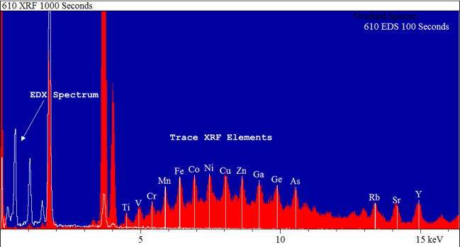
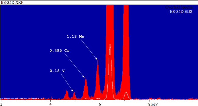
Sensitivity: Steel
XRF can be used for trace spectral acquisition down to low PPM levels. XRF can be 10-1000 times more sensitive than SEM-EDS analysis, exemplified here by the greatly increased trace level peaks in a Brammer B.S.35D steel standard.
Dual Power
These are example maps of both X-ray and electron beam excitation are employed simultaneously on the same sample at the same time! Never before has this ability been demonstrated.
Reference Documents
- Integrated Electron and X-Ray Induced Microbeam XRF in the SEM. Cross BJ, Witherspoon KC. Microscopy Today. Jul;12(4):20-3 (2004).
- Micro-Focus X-Ray Fluorescence (µ-XRF) as an Extension of the Analytical SEM. V.-D. Hodoroaba, et al. Microscopy and Microanalysis. 16(S2):904-905, August 2010.
- Advanced Elemental Analysis with ED-EPMA, WD-EPMA and µ-XRF at a SEM. V.-D. Hodoroaba, et al. Microscopy and Microanalysis 17:600-601, July 2011.
- Comparing the detection of iron-based pottery pigment on a carbon-coated Sherd by SEM-EDS and by Micro-XRF-SEM. Michael Pendleton, et al. The Yale Journal of Biology and Medicine. 87(1):15-20, March 2014.
- Micro-XRF excitation in an SEM. M. Haschke, F. Eggert and W. T. Elam. X-ray Spectrometry. Vol. 36, No. 4, p. 254-259 (2007).
- Micro-XRF in Scanning Electron Microscopes. Michael Haschke and Stephan Boehm. Advances in Imaging and Electron Physics. Vol. 199, p 1-60, (2017).
- A flexible setup for angle-resolved X-ray fluorescence spectrometry with laboratory sources. M. Spanier, C. Herzog, D. Grötzsch, F. Kramer, I. Mantouvalou, J. Lubeck, J. Weser, C. Streeck, W. Malzer, B. Beckhoff, B. Kanngießer. Review of Scientific Instruments, Vol 87, No 3, (035108), (2016).
- Michael Haschke, Laboratory Micro-X-Ray Fluorescence Spectroscopy, Vol. 55 (2014).
- Trends in environmental science using microscopic X-ray fluorescence. Ursula Elisabeth Adriane Fittschen & Gerald Falkenberg. Spectrochimica Acta Part B: Atomic Spectroscopy, Vol 66, No 8, p 567-580 (2011).
- Determination of the real transmission of an X‐ray lens for micro‐focus XRF at the SEM by coupling measurement with calculation of scatter spectra. V.‐D. Hodoroaba & M. Procop. X-Ray Spectrometry, Vol 38, No 3, p 216-221, (2009).
- Improvements of the low‐energy performance of a micro‐focus X‐ray source for XRF analysis with the SEM. X-Ray Spectrometry, Vol 38, No 4, p 308-311, (2009).
- Improvements of the low‐energy performance of a micro‐focus x‐ray source for XRF analysis with the SEM. Procop, Mathias; et al. X‐Ray Spectrometry: An International Journal 38.4 (2009): 308-311.
- A microfocus X-ray source for improved EDS and XRF analysis in the SEM. Procop, Mathias, Vasile-Dan Hodoroaba, and Vanessa Rackwitz. Microscopy and analysis / European edition. p 10-13 (May, 2011).
- X-ray fluorescence as an additional analytical method for a scanning electron microscope. Procop, M., Hodoroaba, V. Microchim Acta Vol 161, p 413–419 (2008).
- Gaining improved chemical composition by exploitation of Compton-to-Rayleigh intensity ratio in XRF analysis. Hodoroaba, Vasile-Dan, and Vanessa Rackwitz. Analytical Chemistry 86.14 (2014): 6858-6864.
- Pendleton, M. W., et al. “Detecting iron-based pigments on ruthenium-coated archaeological pottery by SEM-EDS and by micro-XRF-SEM.” Microscopy and Microanalysis 20.S3 (2014): 2030-2031.
- Rackwitz, Vanessa, et al. “Performance of μ-XRF with SEM/EDS for trace analysis on the example of RoHS relevant elements–measurement, optimisation and prediction of the detection limits.” Journal of Analytical Atomic Spectrometry 28.9 (2013): 1466-1474.
- Sieber, John R., and Adam Mortensen. “Validation and traceability of XRF and SEM‐EDS elemental analysis results for solder in high‐reliability applications.” X‐Ray Spectrometry 43.5 (2014): 259-268.
- Schwandt, C. “Micro XRF Element Maps Are A New Method Of Detecting Elements At Lower Concentrations Than The Electron Beam Produced Corollary: A Garnet Schist Example.” Microscopy and Microanalysis 15.S2 (2009): 34-35.
- 扫描电镜中 扫描电镜中 XRF 与 EDS EDS分析结合 分析结合。陶瓷地矿冶金领域微量元素分析 陶瓷地矿冶金领域微量元素分析 陶瓷地矿冶金领域微量元素分析。
Search Terms
-
- Micro‐XRF excitation in an SEM
- Micro-Focus X-Ray Fluorescence (μ-XRF)
- Micro-XRF-SEM
- Micro‐focus X‐ray source for XRF analysis with the SEM
- Micro‐focus XRF at the SEM
- Micro-XRF in Scanning Electron Microscopes
- µ-XRF at a SEM
- µXRF SEM
- MicroEDXRF SEM
- µEDXRF SEM
- Micro-XRF SEM
- Micro-EDXRF SEM
- Polycapillary SEM
- Poly-capillary SEM
- SEM/XRF
- XRF/SEM
- SEM-XRF
- XRF-SEM
- XRF SEM
- X-ray source SEM
- SEM X-ray source
- X-ray SEM
- X-ray tube SEM
- SEM X-ray
- SEM X-ray tube
- SEM polycap
- polycap SEM
- SEM polycap