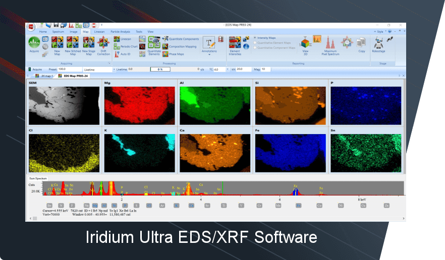
For Scanning Electron Microscopes (SEM), we offer a complete SEM/EDX system: SDD detector, digital signal processor and software. Our all-inclusive, high-end, Windows®-10 based software suite – Iridium Ultra – features a myriad of spectra, mapping, imaging, and advanced automation and analysis tools. IXRF Systems’ SEM/EDS packages deliver premium detector technology as well as both industry-leading and unique (to IXRF) features. No-cost software upgrades are included for the life of the system, so the analyst is never out of date.
Energy Dispersive X-ray Spectroscopy (EDS / EDX)
for Scanning Electron Microscopes (SEM)
SEM/EDS | SEM/EDX
SEM/EDX Overview
Energy-dispersive spectroscopy (EDS, EDX, EDXS or XEDS), sometimes called energy dispersive X-ray analysis (EDXA) or energy dispersive X-ray microanalysis (EDXMA), is an analytical technique used for the elemental analysis or chemical characterization of a sample. It relies on an interaction of an electron beam (e– beam) and a sample within a Scanning Electron Microscope (SEM) instrument. Its characterization capabilities are due in large part to the fundamental principle that each element has a unique atomic structure allowing a unique set of peaks on its electromagnetic emission spectrum (which is the main principle of spectroscopy). The peak positions are predicted by the Moseley’s law with accuracy much better than experimental resolution of a typical SEM/EDS or SEM/EDX instrumentation.
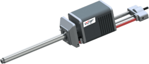
SEM/EDS Electronics
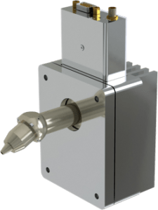
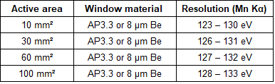
Silicon Drift Detectors (SDD) are available with a choice of window materials, from Beryllium (8µm) to Thin Polymer (for light element x-ray transmission). Sensor active areas of 10mm² to 100mm² are offered. In addition, all or our SDD versions are vibration free.
IXRF’s range of electronically cooled (LN2 free) SDD are optimized when coupled with an innovative Ethernet-based digital pulse processor. Our SDD detectors provide exceptional and stable performance over a wide range of input count rates.
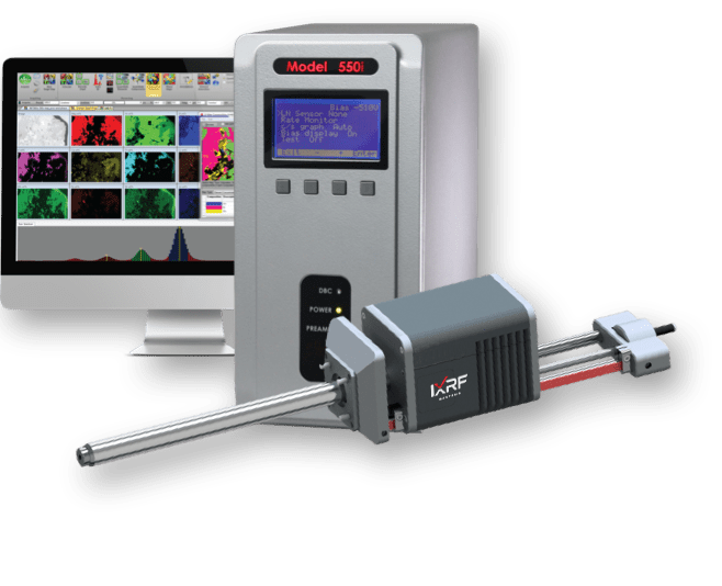
Our Model 550i SEM/EDS digital electronics are optimized for true “data streaming” and ultra-fast X-ray processing. System incorporates Active Imaging combined with Digital Signal Processor (DSP) and a 4096 multi-channel analyzer (MCA).
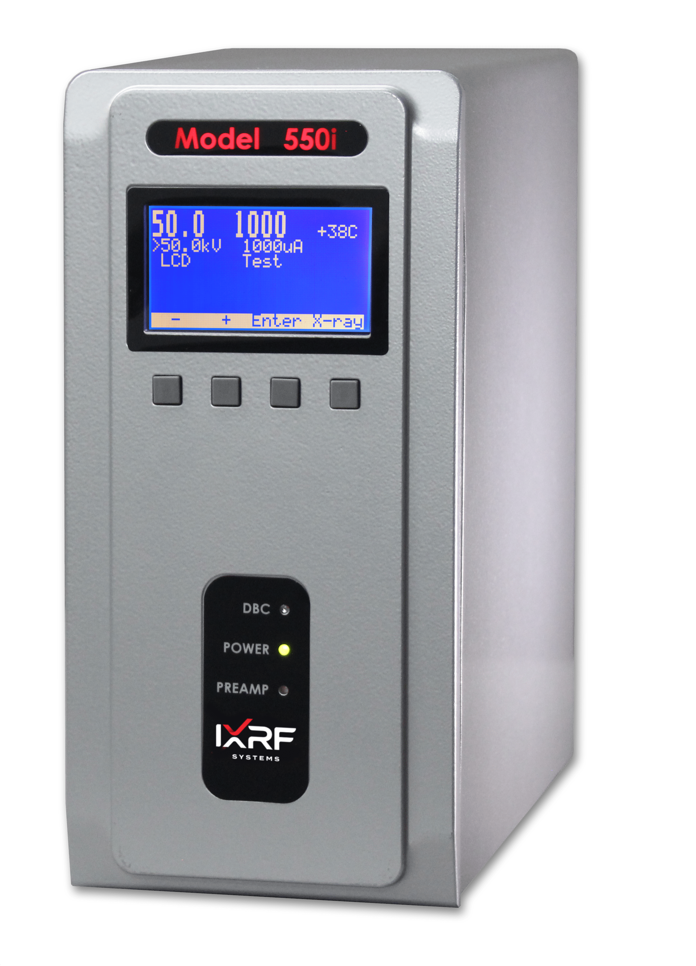
550i Digital Pulse Processor
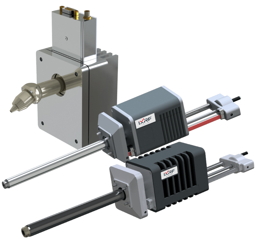
Benchtop
SEM/EDS SDD
Large area
SEM/EDS SDD
Standard
SEM/EDS SDD
IXRF can update your SEM/EDS software and computer to the safety and security of the Windows 10 OS environment. Interoperability with Microsoft Office means generation of reports is simple and intuitive. And your SEM will be compliant with the latest corporate/institutional security protocols.
microXRF X-ray sources for Scanning Electron Microscopes (SEM): addition of an polycapillary X-ray tube and Iridium Ultra software will transform your SEM’s quantitative analytical capabilities. Higher peak to background ratios enable greater elemental sensitivity for higher Z elements: sensitivity exceeding e–-beam excitation by a factor of 10-1000X.
SEM/EDS Overview
- Identifying Elements
- Spectrum Processing
- Annotations
- Spectrum Overlay
- Spectrum Reporting
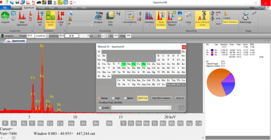
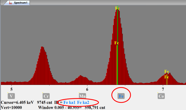
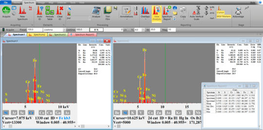
SEM/EDX Indentification
Kα energy markers help easily identify elemental peaks.
Identify elements through cursor ID by selecting individual energy channels.
Automatic peak identification feature.
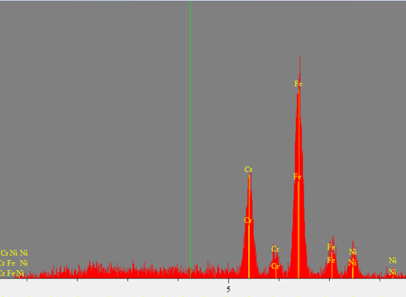
SEM/EDS Processing
• Peak separation using Gaussian deconvolution.
• Automatic peak-overlap correction.
• Automatic escape and sum peak removal.
• Automatic standardless quantification using ZAF.
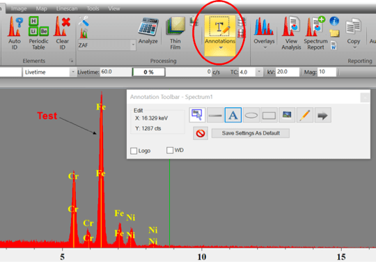
SEM/EDX Annotation
Selecting Annotations from the spectrum toolbar opens a new window that allows the user to measure, label, add text, etc. on the spectrum. These annotations are fully customizable and can be exported with the spectrum.
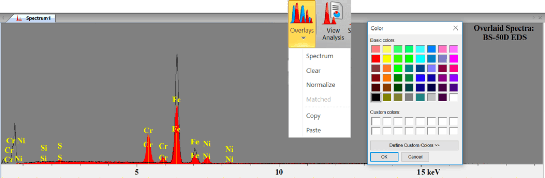
SEM/EDS Spectrum Overlay
Spectra can be overlaid to easily compare the relative compositions in samples.
.
SEM/EDX Reporting
Create spreadsheet reports from multiple spectra’s quantitative analysis results.
SEM/EDS Imaging
- Image Acquisition
- Analysis Suite (Toolbar)
- Morphology
- Segmentation
- Stitching/Montage
- RoboStage
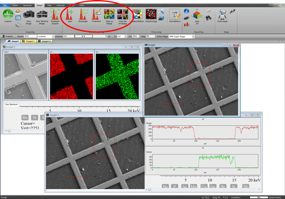
SEM/EDX Direct Acquire
The Direct Acquire tools allow for EDS data to be collected by selecting the region of interest from the SEM image. This includes spot/rectangle/free hand spectra as well as maps and linescans on the image.
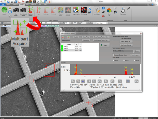
SEM/EDS Multipart
Multipart Acquire allows fully automated spectrum analysis with customized EDS settings and automatically generated spectrum analysis reports. This includes single point, raster area, and freehand line spectrum acquisition.
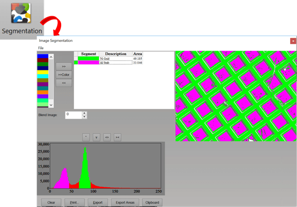
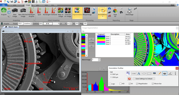
SEM/EDX Segmentation
Image Segmentation provides a visual representation of different phases in an image. Based upon histogram analysis, you can see the percent area each phase occupies.
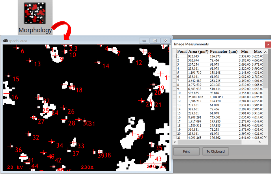
SEM/EDS Morphology
Image Morphology provides particle information through image binarization. Image binarization transforms the image into grayscale based upon histogram data. This allows you to label and measure pixels to provide an abundance of morphological data.
SEM/EDX Segmentation
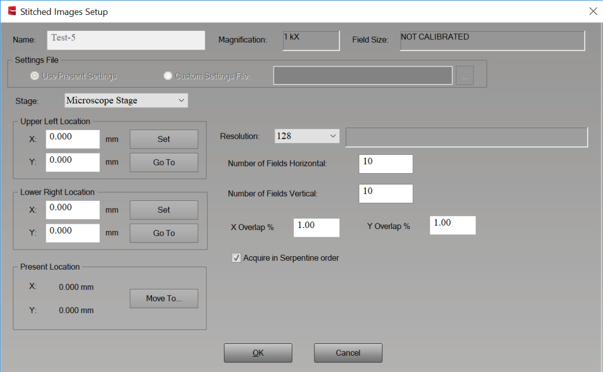
Image and Map stitching allow for acquisition of images/maps over a large area. This is done by moving the stage (automatically or manually) to adjacent fields, forming a grid of images/maps from the data acquired at each field. This grid of images/maps can be stitched together into a single image/map file.
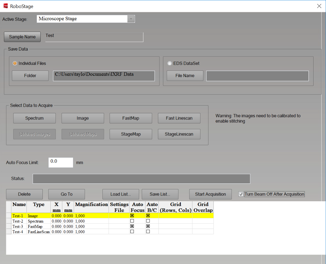
SEM/EDS RoboStage
RoboStage allows unattended acquisition of multiple EDS data from anywhere on the microscope’s stage using the existing stage automation for the microscope to position the stage for each EDS data acquisition. Data are automatically saved in either individual data files or an EDS Dataset file.
SEM/EDS Mapping
- Mutielement Quantitative Mapping
- Overlay Maps
- Map Analysis Suite (Toolbar)
- Extract Spectra (Freehand, Spot, Area)
- Extract Linescan
- DataView (Intensity/Concentration)
- Beam Drift Correction
- Maximum Pixel Spectrum
- Map stitch & montage
- Automate Stage and Beam automation
- Composition Mapping
- Phase Analysis
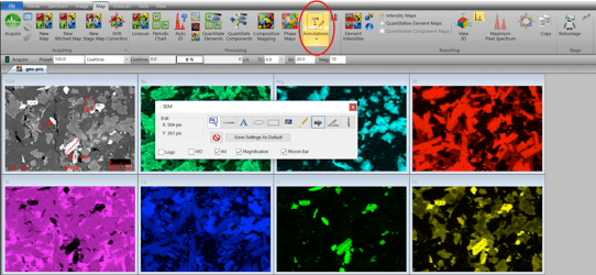
SEM/EDX Annotations
Selecting Annotations from the Map toolbar opens a new window that allows the user to measure, label, add text, etc. on the map.
SEM/EDS: Spectra from Map
Combine X-Ray Map pixels to extract spectra from a region of interest
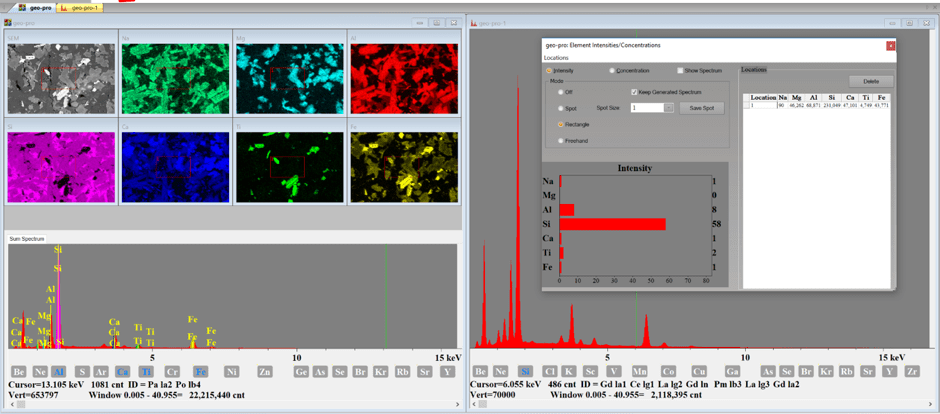
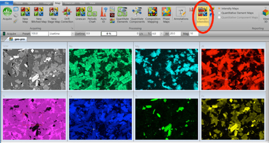
SEM/EDX Intensity Maps
Selecting Element Intensities from the Map tab will open a new window. A spot/rectangle/freehand can be placed on the image to compare the intensity/concentration.
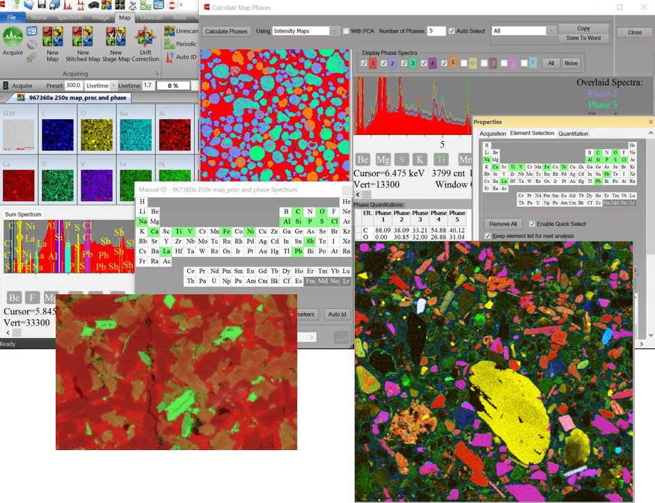
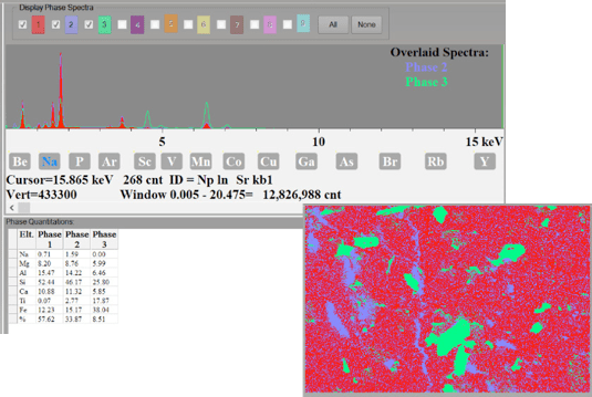
SEM/EDS Phase Maps
Selecting Phase Maps from the Map tab will identify different phases within a sample and quantitatively analyze the elements within each phase.
The different phases will be graphically displayed in a map alongside phase-specific overlaid spectra to provide a qualitative comparison.
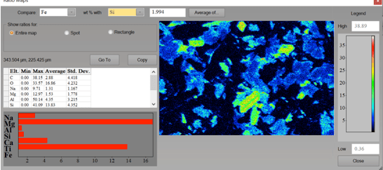
SEM/EDX Ratio Maps
Analyze the element ratios in a region of interest and displays a comparison of element weight percent ratios.
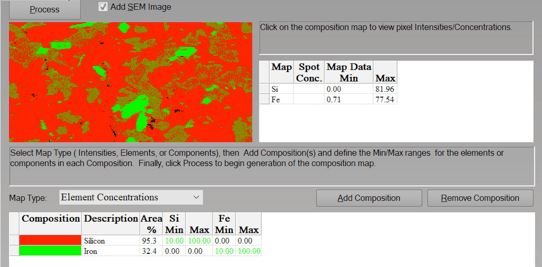
SEM/EDS Composition
Selecting Composition Mapping from the Map tab will identify map locations containing specific element concentrations according to specified parameters.
Quantitative analysis is performed on every pixel where a calculated concentration is compared to a specified concentration. Matching pixels are then displayed in the composition map.
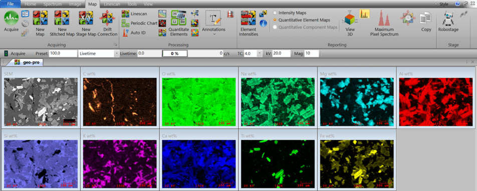
SEM/EDX Quantitative Element / Phase Maps
Quantitative Maps convert the displayed pixel data to Concentration (wt%) from Intensity (cps). This feature can display the quantitative maps as either elemental maps or components maps (ie; oxides).
SEM/EDX Linescans
- Multielement Linescan Acquisition
- Linescan Overlay
- DataView (Intensity/Concentration)
- MultiScan
SEM/EDS Multielement Scan
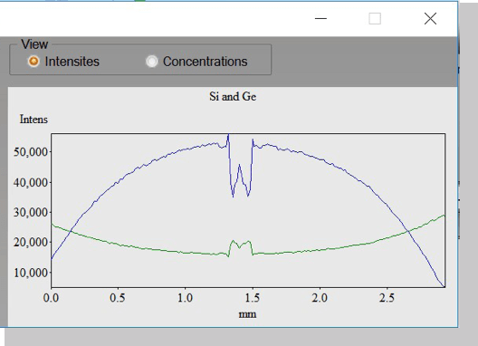
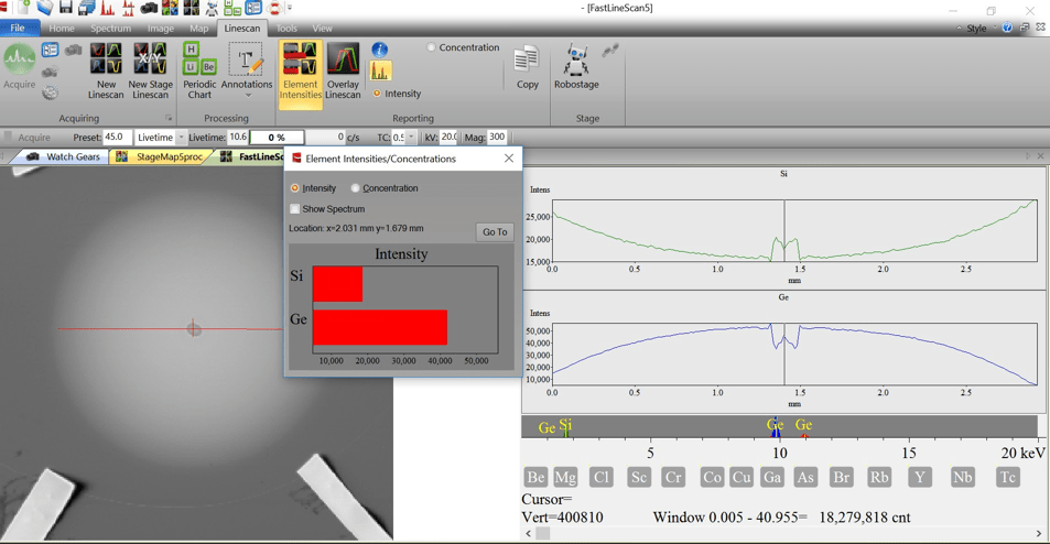
In SEM/EDS, X-ray linescans are excellent tools for determining the location of phases, particles, and other features on a sample that can be discriminated by variations in elemental composition. An X-ray linescan is performed by acquiring XRF data at evenly spaced points along a horizontal line on the sample. The intensity or concentration data are displayed on the screen as line graphs, one for each element in the element list for the linescan.
SEM/EDX Overlay Scans
In SEM/EDX, linescans can be combined and overlaid on the SEM image using the View/Overlay Linescans menu item. Click on the Overlay On Image button to copy the combined graph onto the image. At right is an example of a graph overlaid on the image as an annotation. The graph can be moved, sized, and deleted using the Edit/Annotations panel for the image. The graph can be moved, but will always retain its alignment to the location that the linescan was acquired.
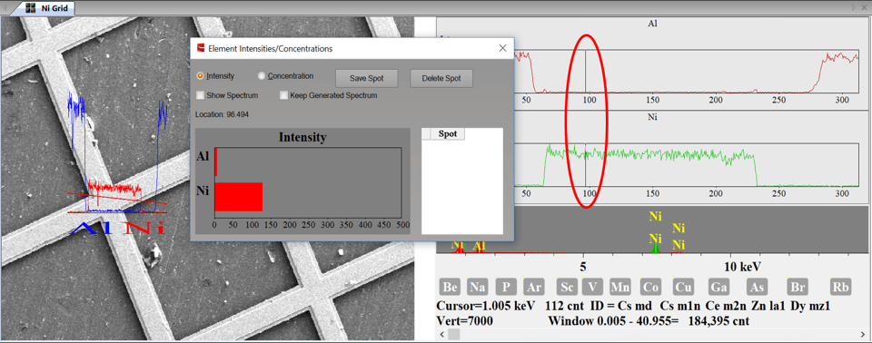
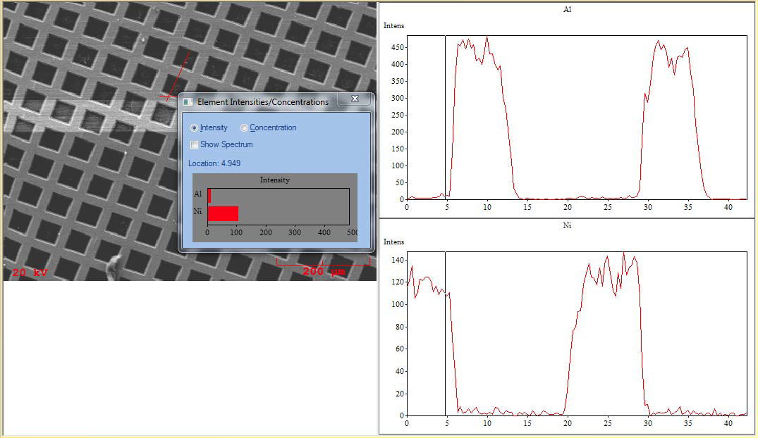
SEM/EDS Dataview
Select View/Intensities Concentrations from the menu to inspect the x-ray data at individual points on the linescan. This insert panel will appear. Click anywhere on a linescan to select a point to inspect the X-ray intensities, as shown. The panel now displays a histogram of the intensity of each element at the selected point. Selecting Concentration in the panel will apply ZAF corrections to the intensities and re-display the histogram with the calculated values as weight percent.
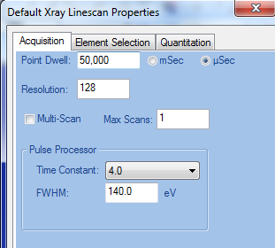
SEM/EDX MultiScan
MultiScan acquires multiple scans of the line of the linescan. The scans are summed together, producing ever-increasing quality in the linescan as the scans are acquired. MaxScans is the maximum number of scans that will be acquired. The acquisition can be stopped at any time, allowing the user to determine when the linescans are of sufficient quality. The advantages of performing the linescan with MultiScan are: 1.) the linescan can be stopped at any time, and 2.) sample charging effects are minimized due to the rapid movement of the beam over the line being acquired.
Energy Dispersive X-ray Spectroscopy (SEM/EDS)
Energy-dispersive X-ray spectroscopy (EDS, EDX, EDXS or XEDS), sometimes called energy dispersive X-ray analysis (EDXA) or energy dispersive X-ray microanalysis (EDXMA), is an analytical technique used for the elemental analysis or chemical characterization of a sample. It relies on an interaction of some source of X-ray excitation and a sample. Its characterization capabilities are due in large part to the fundamental principle that each element has a unique atomic structure allowing a unique set of peaks on its electromagnetic emission spectrum[2] (which is the main principle of spectroscopy). The peak positions are predicted by the Moseley’s law with accuracy much better than experimental resolution of a typical EDX instrument.
SEM/EDX Theory of Operation
Energy Dispersive X-Ray Spectroscopy (EDS or EDX) is a chemical microanalysis technique used in conjunction with scanning electron microscopy (SEM). The EDS technique detects x-rays emitted from the sample during bombardment by an electron beam to characterize the elemental composition of the analyzed volume. Features or phases as small as 1 µm or less can be analyzed.
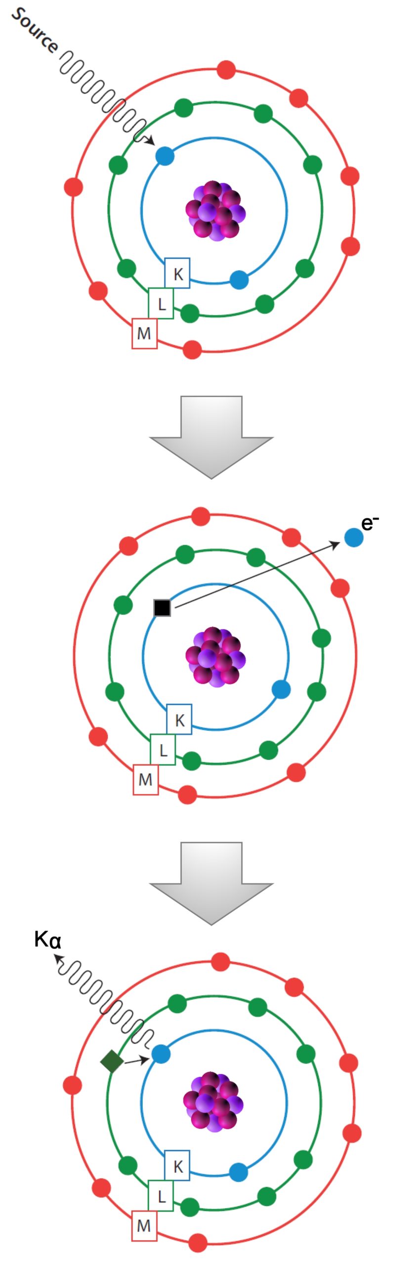
When a sample is bombarded by a SEM’s electron beam (top image), inner shell electrons may be ejected from atoms at the sample’s surface (center image). The energy of the SEM electron (e–) beam must be greater than the energy with which the inner shell electron is bound to the nucleus of the atom. When an inner orbital electron is ejected from an atom, an electron from a higher energy level orbital will be transferred to the lower energy level orbital. During this transition a photon may be emitted from the atom. This fluorescent light (Kα) is the characteristic X-ray of the element (bottom image). The energy of the emitted photon will be equal to the difference in energies between the two orbitals occupied by the electron making the transition. Because the energy difference between two specific orbital shells, for a given element, is always the same (i.e. characteristic of that particular element), the photon emitted when an electron moves between these two levels will always have the same energy. Therefore, by determining the energy (keV) of the X-ray light (photon) emitted by a particular element, it is possible to determine the identity of that element.
For a particular energy (keV) of fluorescent light emitted by an element, the number of photons per unit time (generally referred to as peak intensity or count rate) is related to the amount of that analyte in a sample. The counting rates for all detectable elements within a sample are usually calculated by counting, for a set amount of time, the number of photons that are detected for the various analytes’ characteristic X-ray energy lines. Therefore, by determining the energy of the X-ray peaks in a sample’s spectrum, and by calculating the count rate of the various elemental peaks, it is possible to qualitatively establish the elemental composition and to quantitatively measure the concentration of those elements.
The EDS X-ray sensor measures the relative abundance of emitted X-rays versus their energy. Today sensors are typically Peltier-cooled, solid-state silicon drift detector (SDD) devices. When an incident X-ray strikes the detector, it creates a charge pulse that is proportional to the energy of the x-ray. The charge pulse is converted to a voltage pulse (which remains proportional to the x-ray energy) by a charge-sensitive pre-amplifier. The signal is then sent to a multichannel analyzer where the pulses are sorted by voltage. The energy, as determined from the voltage measurement, for each incident X-ray is sent to a computer for display and further data evaluation. The spectrum of x-ray energy versus counts is evaluated to determine the elemental composition of the sampled volume.
On-line SEM/EDS Microanalysis Course
Electron Probe Micro Analysis Course Materials
Lecture Notes
- Title Page
- Chapter 1 Introduction
- Chapter 2 Specimen Interactions
- Chapter 3 Nature of X-rays
- Chapter 4 Electron Optics
- Chapter 5 Wavelength Dispersive Spectrometry
- Chapter 6 Energy Dispersive Spectrometry
- Chapter 7 Statistics
- Chapter 8 Mapping and Imaging
- Chapter 9 Matrix Corrections
Power Point Files (By Lecture Number)
- Introduction to the EPMA/SEM laboratory: An introduction to the technique followed by a short tour of the facilities and including discussion of lecture notes, suggested reading materials, grading methods, exams and current research projects followed by a short history of the instrument and related techniques.
- Electron beam instrumentation and electron solid interactions: A brief description of the major system components for both the electron microprobe and scanning electron microscope followed by an introduction to elastic and inelastic scattering of electrons and associated principles. (chapters 1 and 2)
- X-ray productions: The generation and emission of characteristic and continuum x-rays and their absorption and fluorescence interactions within the sample. (chapter 3)
- Electron Beam Columns: Formation, alignment, and choices for parameterization with regards to application and specimen interaction. (chapter 4)
- Lab: Demonstration of electron beam parameters and sample interactions.
- WDS (wavelength dispersive spectrometery): A description of the Bragg spectrometer and associated principles. (chapter 5)
- Lab: Demonstration of wavelength dispersive spectrometry technique and analysis.
- EDS (energy dispersive spectrometery): Spectral analysis using the EDS detector. (ch. 6)
- Lab: Demonstration of energy dispersive spectrometry technique and analysis.
- Statistics: The essential key to scientific analysis. (chapter 7)
- Lab: Examples of the application of statistical calculations to quantitative analysis.
- Quantitative matrix corrections: What goes on in the computer? An introduction to the corrections being applied to the intensity data in order to obtain elemental concentrations. Take home mid-term exam given out at the end of the lecture and due next class meeting. (chapter 9). See also this PPT on standard accuracy by John Fournelle.
- Digital Imaging (Lecture and Lab): Imaging and mapping: An overview of electron and x-ray imaging and mapping techniques and the principles involved along with a demonstration of the analog and digital mapping capabilities on the electron microprobe.
- Volz, Heather M., et al. Development of a macroscopic quantitative x-ray fluorescence capability to study heterogeneities in cast uranium alloys. No. LA-UR-10-02375; LA-UR-10-2375. Los Alamos National Lab.(LANL), Los Alamos, NM (United States), 2010.
-
Scipioni, Larry, Lewis Stern, and John Notte. “Applications of the helium ion microscope.” Microscopy Today 15.6 (2007): 12-15.
- Bode, Michael. “The Case For Digital Imaging.” Microscopy Today 7.8 (1999): 23-25.
- Atomic spectrometry update: review of advances in the analysis of metals, chemicals and functional materials. Carter, Simon; Fisher, Andy; Garcia, Raquel; Gibson, Bridget; Marshall, John; Whiteside, Ian. JAAS (Journal of Analytical Atomic Spectrometry). Nov2016, Vol. 31 Issue 11, p2114-2164. 51p. DOI: 10.1039/c6ja90044e.
Reference Documents
- Feng, L., V. D. Saveliev, M. Takahashi, C. R. Tull, S. Barkan, E. V. Damron, S. Kosuge, R. D. Lamb, K. C. Witherspoon, and Per O. Sjoman. “An Improved Large Area Silicon Drift Detector EDS System for Low Energy X-ray Detection and Fast Spectrum Imaging.” Microscopy and Microanalysis 15, no. S2 (2009): 174-175.
- Cross, Brian John, and K. C. Witherspoon. “Integrated XRF in the SEM.” Microscopy and Microanalysis 10.S02 (2004): 104.
- Newbury*, Dale E., and Nicholas WM Ritchie. “Is scanning electron microscopy/energy dispersive X‐ray spectrometry (SEM/EDS) quantitative?” Scanning 35.3 (2013): 141-168.
- Martiny, Andrea, et al. “SEM/EDS analysis and characterization of gunshot residues from Brazilian lead-free ammunition.” Forensic Science International 177.1 (2008): e9-e17.
- Newbury, Dale E., and Nicholas WM Ritchie. “Elemental mapping of microstructures by scanning electron microscopy-energy dispersive X-ray spectrometry (SEM-EDS): extraordinary advances with the silicon drift detector (SDD).” Journal of Analytical Atomic Spectrometry 28.7 (2013): 973-988.
- Gazulla, M. F., et al. “Nitrogen determination by SEM‐EDS and elemental analysis.” X‐Ray Spectrometry 42.5 (2013): 394-401.
- Akkaş, Efe, et al. “Application of decision tree algorithm for classification and identification of natural minerals using SEM–EDS.” Computers & Geosciences 80 (2015): 38-48.
-
Wilkinson, Kai, et al. “New tabletop SEM-EDS-based approach for cost-efficient monitoring of airborne particulate matter.” Environmental Pollution 159.1 (2011): 311-318.
- Figueiredo, Elin, et al. “Inclusions and metal composition of ancient copper‐based artefacts: a diachronic view by micro‐EDXRF and SEM‐EDS.” X‐Ray Spectrometry 40.5 (2011): 325-332.
- Ramirez-Leal, Roberto, Maryanna Valle-Martinez, and Martin Cruz-Campas. “Chemical and morphological study of PM10 analysed by SEM-EDS.” Open Journal of Air Pollution 3.04 (2014): 121.
- Goldstein, J. I., Newbury, D. E., Michael, J. R., Ritchie, N. W., Scott, J. H. J., & Joy, D. C. (2017). Scanning electron microscopy and X-ray microanalysis. Springer.
- https://en.wikipedia.org/wiki/Electron_microscope
- https://en.wikipedia.org/wiki/Scanning_electron_microscope
- https://en.wikipedia.org/wiki/Energy-dispersive_X-ray_spectroscopy
Search Terms
-
- EDS
- EDX
- EDXS
- XEDS
- EDXA
- EDXMA
- SEM/EDS
- SEM/EDX
- SEM/EDXS
- SEM/XEDS
- SEM/EDXA
- SEM/EDXMA
- Energy dispersive X-ray analysis
- Energy-dispersive spectroscopy
- Energy-dispersive X-ray spectroscopy
- Energy dispersive X-ray microanalysis
- X-ray microanalysis
- Microanalysis
- Micro-analysis
- X-ray micro-analysis
- SEM X-ray microanalysis
- SEM micro-analysis
- SEM X-ray micro-analysis
- SEM microanalysis
- SEM-EDS
- SEM-EDX
- SEM-EDXS
- SEM-XEDS
- SEM-EDXA
- SEM-EDXMA
- Energy dispersive X-ray analysis
- Electron microscopy
- Scanning electron microscopy
ABSTRACT
In the 50 years since the first mating of semiconductor-based energy-dispersive X-ray spectrometry (EDS) with the scanning electron microscope (SEM), this hybrid instrument has become an indispensable microanalytical tool. In the last two decades a new detector, the silicon drift detector (SDD), has overtaken earlier Si(Li) technology and has made EDS in the SEM and TEM faster and better. This article tells the story of the SDD development and describes improvements in count rate capability, energy resolution, and detector geometry that bring to SEM microanalysis exceptional precision and stability. Quality maps of element distributions can now be obtained in minutes instead of hours.

SEM/EDS Applications
Archeology/Museums
Museum artifacts and currency
Metals and alloys
Gemstone inclusions
Painting authenticity/dating
Paints, inks, pigments
Corrosion products
Biomedical devices/implants
Solar cells
Optical filters
Manufacturing
Pathology
Pharmaceuticals
Semiconductor
RoHS, WEEE, and ELV compliance
Geological
Meteorites
Phase boundaries
Mineral identification
Mining test cores
Electronics
Glasses
Building materials (concrete, cement)
Packaging
Medicine/Biology
Bones/tissue
Leaves/plants
Implants
Particle Analysis
Environmental analysis
Lead contamination in consumer goods
Soil contamination
Material characterization for recycling
Marine/ocean sediments
Airborne particles/air filters
Slurry
Forensic Science
Glass Chips
Paint cross sections
Inks/pigments
Soils/stones
Gun shot residue
Material identification