In the realm of semiconductor manufacturing, the homogeneity of Sn (Tin), Ti (Titanium), and Co (Cobalt) deposition is crucial. This is not limited to techniques like DC magnetron sputtering but extends across several deposition methods. The uniformity of these elements significantly impacts the performance, reliability, and longevity of semiconductor devices for several reasons:
Consistency in Electrical Properties: In semiconductor devices, the uniformity of the deposited materials heavily influences electrical properties like conductivity and resistivity. For instance, uneven deposition of Sn, Ti, and Co can lead to irregularities in the electrical characteristics of the semiconductor devices, which may result in device failure or reduced efficiency.
Structural Integrity and Performance: The physical and mechanical properties of the thin films, including their strength and adherence to the substrate, depend on the uniformity of the deposition. Non-homogeneous layers can lead to weak spots, increasing the likelihood of physical degradation or failure under stress.
Optimization of Optical Properties: For semiconductor devices that rely on optical properties, like photovoltaic cells or sensors, the uniformity of the deposited layers is essential. Variations in layer thickness can affect the absorption and reflection of light, impacting the device’s performance.
Enhanced Reliability: Uniform deposition ensures consistent quality across the entire wafer, improving the semiconductor devices’ reliability. This is particularly important in high-performance and critical applications like aerospace, military, and medical devices.
Process Control and Yield: Monitoring homogeneity helps fine-tune the deposition process, leading to better control over the manufacturing process. This improves the quality of the end product and enhances the overall yield, reducing waste and manufacturing costs.
Diverse Deposition Techniques in Semiconductor Fabrication
Semiconductor fabrication employs various deposition methods beyond DC magnetron sputtering. These include Chemical Vapor Deposition (CVD), Atomic Layer Deposition (ALD), Electroplating, and Molecular Beam Epitaxy (MBE). Each technique has unique advantages and is chosen based on the specific requirements of the manufactured semiconductor device.
Analytical Methods for Monitoring Deposition Homogeneity
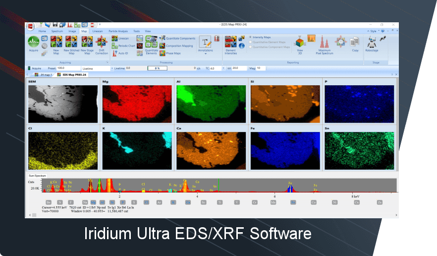
Accurate monitoring of deposition homogeneity is essential across all these techniques. This is where analytical methods like microXRF (Micro X-ray fluorescence) play a pivotal role in ensuring the uniform application of materials and identifying any deviations in thickness or composition that could affect device performance. These spectrometers, such as the ATLAS series from IXRF Systems, are designed for hyperspectral imaging and elemental analysis from carbon (C) to uranium (U). They are known for their high-end micro-spot X-ray fluorescence capabilities with an X-ray beam size as small as 5 µm, providing very high spatial resolution.


Figure 1: (Image 1) Three-inch combinatorial wafer post-sputtering, post-annealing. (Image 2-4) Overlay Micro XRF intensity map of the wafer displaying the distribution of Ti, Co, & Sn. These maps were obtained using a 25 μm spot size.


Figure 2: (Image 1-3) Individual quantitative microXRF maps of a wafer seen above, displayed as thermal heat maps, showcasing the distribution and uniformity of Sn, Co, and Ti, respectively.
The ATLAS SEMI, specifically, is tailored for semiconductor metrology, providing detailed analysis capabilities necessary for the semiconductor industry. This includes the analysis of bump inspection, film stack, multi-stack structures, and Sn/Ag bump/pillar measurements. The system can analyze for corrosion resistance coating, thickness and composition control, and even under bump metallization (UBM), which are crucial for the fabrication of integrated circuits and other semiconductor devices.
MicroXRF, with its non-destructive measurement technique and superior trace element sensitivity, can significantly assess the homogeneity of Sn, Ti, and Co deposition. It offers the advantage of analyzing a wide range of elements with high precision and over a large area, which ensures the uniformity of thin films in semiconductor applications. Additionally, the ATLAS M microXRF Spectrometer features up to 4 Silicon Drift Detectors (SDD) for increased precision and reduced acquisition times. It can perform high-resolution mapping with a 5 μm spot size. This makes it particularly useful for the analysis of small features or variations in composition across a wafer.
Conclusion
In summary, IXRF’s microXRF systems play a significant role in the semiconductor industry due to their high-resolution capabilities and sophisticated software for data analysis. These systems are valuable for the detailed analysis of thin films, which is a crucial aspect of quality control and development in semiconductor device manufacturing. Furthermore, the importance of maintaining the homogeneity of Sn, Ti, and Co depositions cannot be overstated in the context of producing consistent and reliable semiconductor devices. MicroXRF techniques are well-suited for this task, offering the necessary precision and resolution for effective monitoring and quality control within these processes.
Explore semiconductors with the Atlas from IXRF Systems
Interested in enhancing the quality and reliability of your semiconductor devices? IXRF Systems offers advanced microXRF spectrometers designed for precise thin film analysis. Connect with our team to explore how our technology can cater to your specific needs in semiconductor manufacturing. Contact us to schedule a discussion and discover how IXRF’s solutions can contribute to your success.