Accurate and efficient analysis is paramount in microelectronics. Microelectronics is the backbone of modern technology, powering everything from smartphones and laptops to medical devices and aerospace innovations. As the industry continues to evolve, so does the need for cutting-edge analytical methods. Enter microX-ray fluorescence (MicroXRF, microEDXRF, µXRF, µEDXRF), a non-destructive and powerful technique redefining how electronics are analyzed.
What is MicroXRF?
MicroXRF is a non-destructive analytical method that uses focused X-ray radiation to determine a sample’s elemental composition. When a sample is exposed to a focused X-ray beam, its atoms absorb the energy and re-emit it as characteristic X-ray fluorescence. This process provides detailed information about the elements present within the sample.
The term “Micro” in MicroXRF highlights its ability to focus on exceptionally small areas, with systems like the Atlas series, which has a spatial resolution as small as a 5 µm spot diameter. This precision enables high-resolution elemental mapping, making it ideal for analyzing the intricate features of microelectronic components.
Applications of MicroXRF in Microelectronics
MicroXRF supports various applications in the microelectronics sector, from quality control to failure analysis.
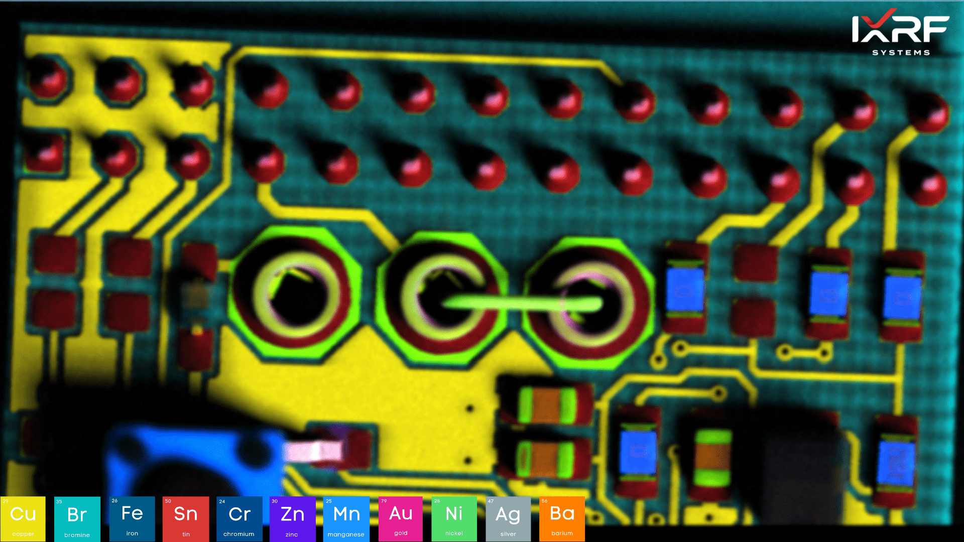
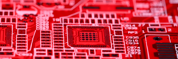
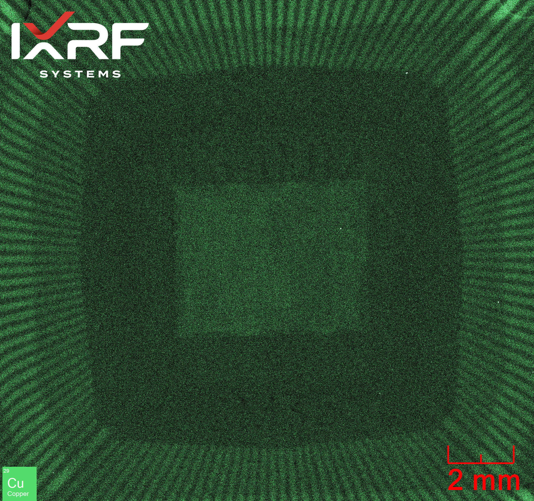
Figure 1. A 2D elemental map of a printed circuit board (PCB) illustrating the non-destructive elemental analysis technique.


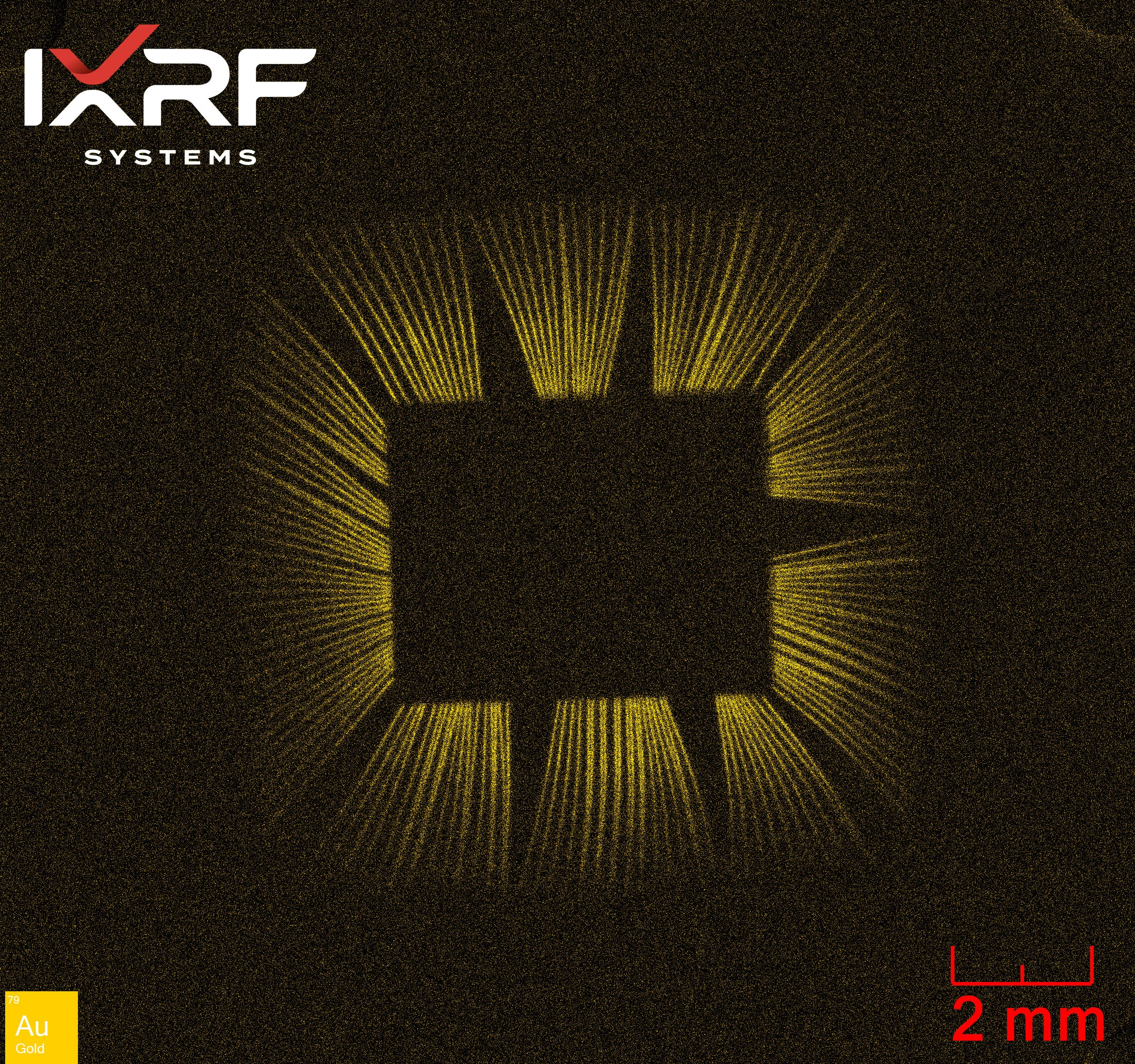
Figure 2: A 2D elemental map and submap of an integrated circuit, quad flat package (QFP) analyzed with intact packaging.
Here’s a closer look at its capabilities:
1. Quality Control
Maintaining strict quality standards is essential in microelectronics manufacturing. MicroXRF allows manufacturers to:
- Inspect incoming materials for compliance with specifications.
- Perform routine inspections during production to ensure consistent quality.
- Detect impurities, such as substandard solder used in circuit boards, to ensure reliability.
2. Failure Analysis
When components fail, determining the root cause is critical. MicroXRF excels at:
- Analyzing failed components for material defects or design flaws.
- Identifying specific issues, such as elemental inconsistencies, that contribute to failures.
- Providing actionable insights to prevent future malfunctions.
3. Material Characterization
Understanding the composition of materials used in microelectronics is vital for innovation. MicroXRF can:
- Characterize conductive materials for optimized electrical properties.
- Aid in developing new materials and enhancing existing ones for specialized applications.
4. Coating Analysis
Thin coatings play a crucial role in device performance and durability. MicroXRF enables:
- Precise measurement of coating thickness.
- Assessment of coating uniformity and composition.
- Analysis of materials crucial for protecting and enhancing electronic components.
5. Research and Development
Innovation in microelectronics relies on exploring new materials and structures. MicroXRF supports R&D by:
- Providing detailed elemental data to guide material selection.
- Enabling the development of novel components with enhanced properties.
6. Process Development
MicroXRF plays a significant role in optimizing manufacturing processes by:
- Analyzing samples at different production stages.
- Identifying inefficiencies or deviations in processes.
- Ensuring high-quality output through continuous monitoring.
7. Environmental Monitoring
Complying with environmental standards like the RoHS Directive is critical. MicroXRF can:
- Detect hazardous materials, such as lead or cadmium, in electronic components.
- Support the design of eco-friendly electronics by ensuring compliance with regulations.
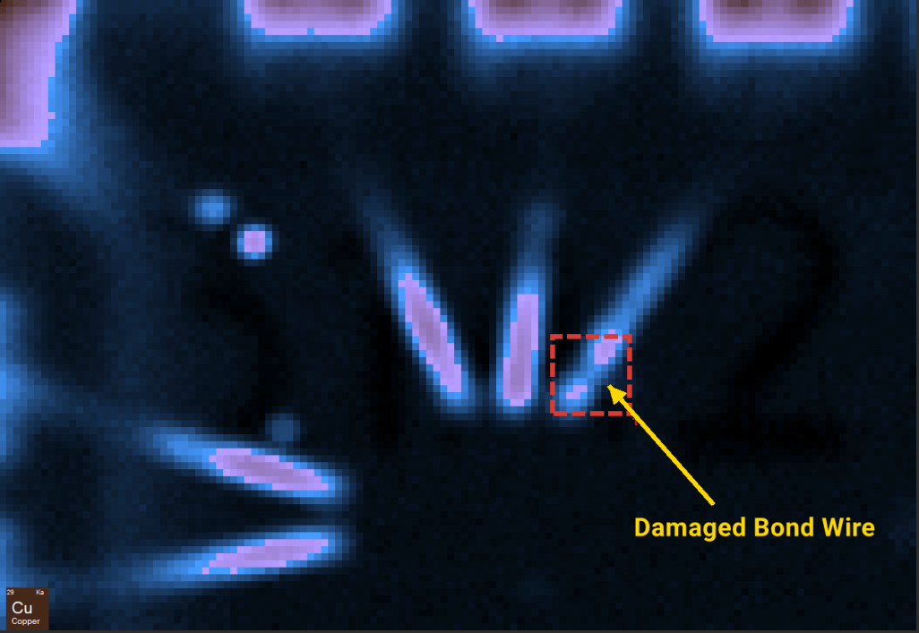
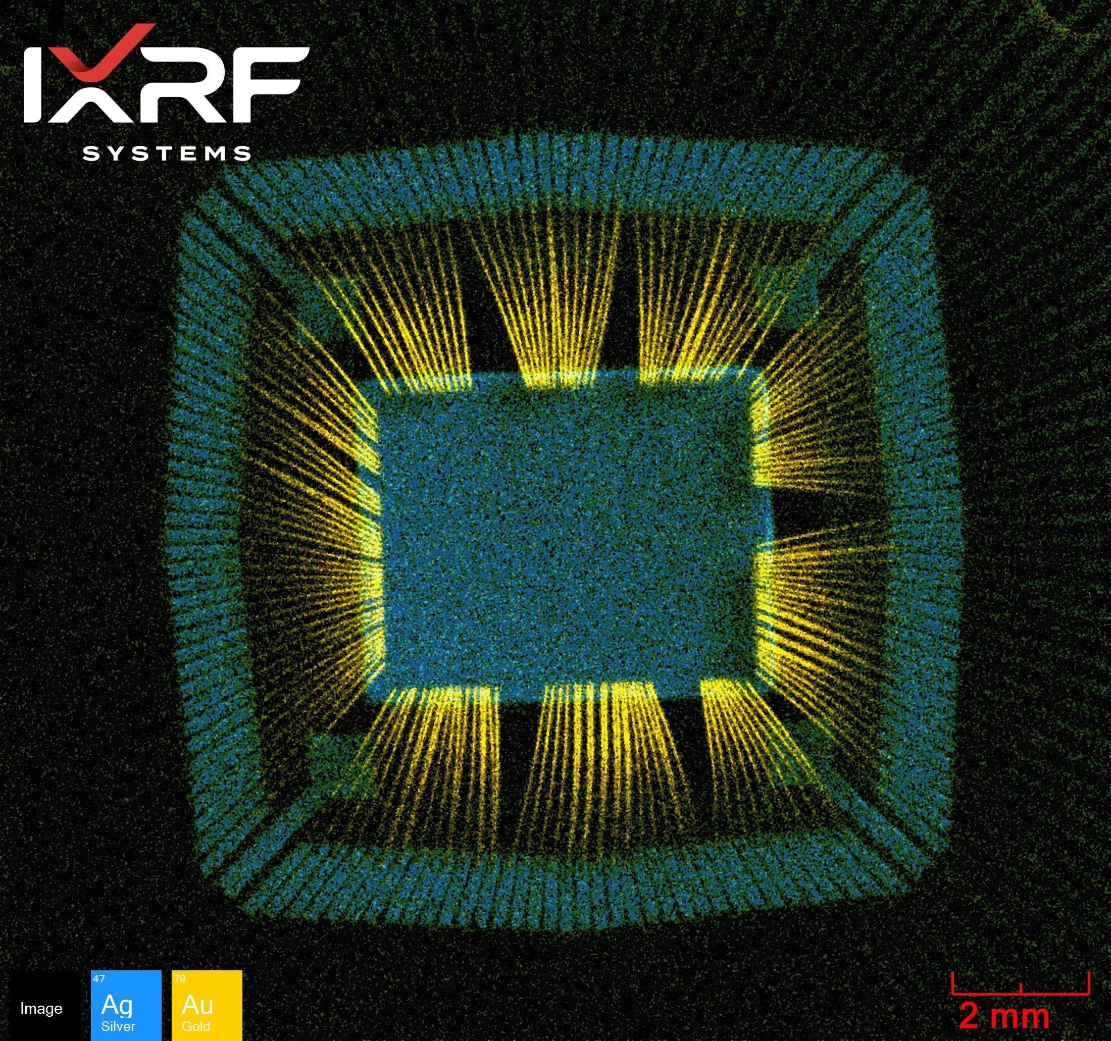
Figure 3: A 2D elemental map of an integrated circuit, ball grid array (BGA) analyzed with intact packaging identifying a damaged wire bond caused by laser etching.
Why Choose MicroXRF for Microelectronics?
MicroXRF stands out as a versatile analytical solution tailored to the needs of modern microelectronics. Whether it’s ensuring product quality, preventing failures, or driving innovation, MicroXRF delivers precise and reliable results.
Conclusion
As microelectronics continue to shrink in size and grow in complexity, the demand for accurate, non-destructive analysis techniques like MicroXRF is set to rise. Its unparalleled ability to analyze small areas, combined with its versatility across quality control, R&D, and environmental monitoring, positions MicroXRF as an essential tool for ensuring the reliability and performance of next-generation microelectronic components.
Key Takeaways
- MicroXRF is a non-destructive, high-resolution technique for analyzing elemental composition.
- It is essential for applications like quality control, failure analysis, and coating characterization in microelectronics.
- MicroXRF supports sustainable practices by identifying hazardous materials in compliance with environmental regulations.
By integrating MicroXRF into microelectronics workflows, engineers and researchers can unlock new levels of precision, efficiency, and innovation.
