Electron microscope analyzers, built for the elements you need to see
SEM/EDS and SEM-XRF systems that attach to any scanning electron microscope, from any major brand, and are engineered and built in the USA.
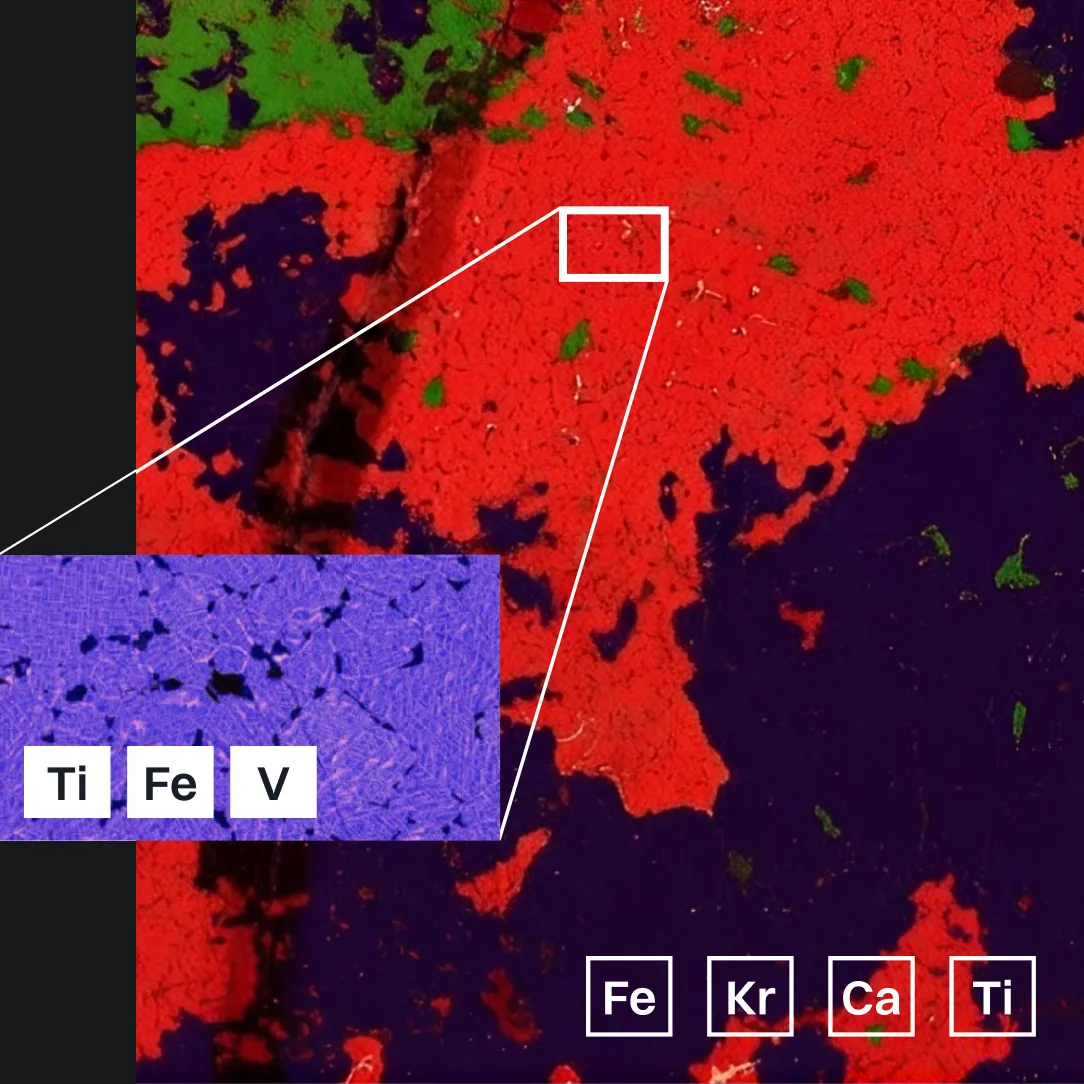
One vendor. One platform. Two ways to see composition.
EDS handles routine elemental ID at the point of the electron beam. SEM-XRF adds a micro-spot X-ray source to the same SEM, extending element coverage, trace sensitivity, and non-destructive depth that EDS alone can't reach.
1
Only vendor offering both from one platform
EDS and SEM-XRF, sold and supported by the same company.
2
Compatible with all major SEM brands
Retrofits onto the SEM your lab already owns.
3
Designed and made in the USA
Iridium Ultra software, detector, and DSP built in-house.
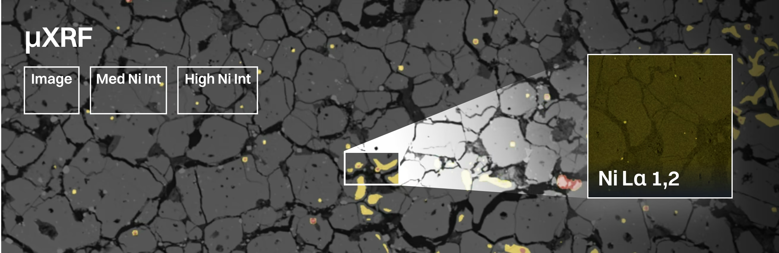
EDS, SEM-XRF, Detectors, and Software for Any SEM
Detectors, micro-spot X-ray sources, software, and upgrades that extend the SEM your lab already owns — from one vendor.
SEM/EDS
Energy-dispersive X-ray spectrometry for any SEM — detector, DSP, and Iridium Ultra software.
SDD Detectors
Silicon drift detectors sized and configured for your SEM chamber.
SEM/MicroXRF
The Xb micro-spot X-ray source — full microXRF capability added to any SEM.
EDS Software
Iridium Ultra — acquisition, quantification, mapping, and phase classification.
Upgrades
Add SEM-XRF to an existing EDS installation, or refresh an aging detector.
Where EDS and SEM-XRF Work Together
Application areas where pairing EDS with SEM-XRF resolves what either technique alone can miss.
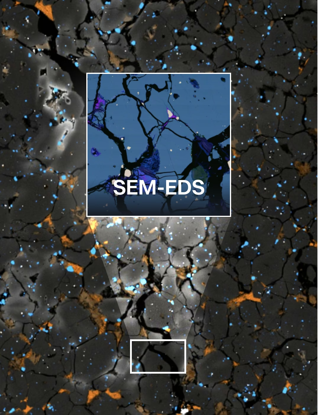
Alloys, Coatings, and Phase Mapping
Resolve compositional gradients and phase boundaries that small-area EDS alone can miss.
Also used for:
- Wafer and die-level screening
- Ore characterization and phase ID
- Trace evidence, court-ready
- Electrode and cell composition
- Interconnects and contamination
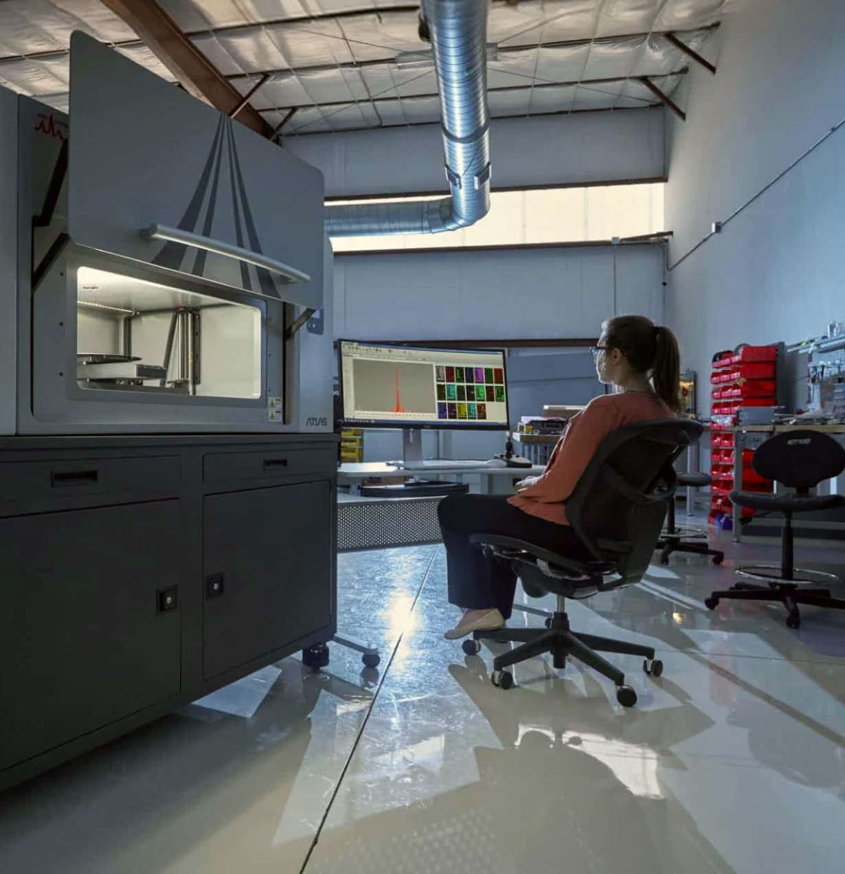
Fits the SEM You Already Have
IXRF EDS and SEM-XRF systems install on all major SEM brands, so you're not locked into a single microscope vendor to get both techniques.








Not sure which system
fits your samples?
Send us your application and we'll recommend an EDS, SEM-XRF, or combined configuration.
Frequently
Asked Questions
SEM-EDS combines a scanning electron microscope with energy-dispersive X-ray spectroscopy to identify and measure the elements present in microscopic features. The SEM electron beam excites atoms in the sample, producing characteristic X-rays that the EDS detector uses for qualitative and quantitative elemental analysis.
Yes. IXRF EDS systems can be integrated with many existing scanning electron microscopes, allowing laboratories to add or modernize elemental-analysis capabilities without replacing the SEM. Compatibility depends on the microscope model, available detector ports, geometry, electronics, and system configuration.
IXRF EDS systems can be integrated with a wide range of SEM platforms from major microscope manufacturers. Compatibility is evaluated based on the specific SEM model, detector-port configuration, chamber geometry, stage clearance, and available interfaces.
IXRF SEM-EDS systems can detect a broad range of elements, including light elements such as boron, carbon, nitrogen, oxygen, and fluorine, as well as transition metals and heavier elements. Detectable range depends on detector configuration, SEM operating conditions, and sample composition.
Yes. IXRF can provide new EDS detectors, electronics, computers, and analytical software for compatible SEMs with older, unsupported, or underperforming EDS systems. An upgrade can improve sensitivity, acquisition speed, software capabilities, and overall analytical performance while extending the useful life of the microscope.
Yes. SEM-EDS can create elemental maps, spectra, linescans, and quantitative composition measurements from microscopic regions of interest. Elemental mapping is particularly useful for identifying phases, contaminants, inclusions, interfaces, and compositional differences across complex materials.
IXRF offers silicon drift detectors in multiple active-area and window configurations to balance count rate, light-element sensitivity, spectral performance, and available SEM geometry. The appropriate detector is selected based on the microscope, applications, elements of interest, and required analytical throughput.
SEM-EDS is widely used to analyze metals, minerals, ceramics, semiconductors, electronic components, coatings, particles, composites, geological materials, and other solid materials. Conductive coating or other sample preparation may be required depending on the SEM, vacuum conditions, and material being examined.
SEM-EDS provides very high spatial resolution for analyzing microscopic features, while microXRF is better suited to larger samples and mapping areas, greater X-ray penetration, and many trace-element applications. Used together, the techniques provide complementary elemental information from the microscale to much larger sample areas.
IXRF EDS systems include Iridium Ultra™ integrated software for spectrum acquisition, element identification, quantitative analysis, elemental mapping, linescans, image correlation, and data review. The software is designed to bring SEM imaging and elemental-analysis workflows together in a single analytical environment.