SEM/MicroXRF: Full Elemental Coverage Beyond What EDS Alone Can Reach
IXRF's Xb micro-spot X-ray source adds a complete micro X-ray fluorescence spectrometer to a scanning electron microscope. Higher peak-to-background ratios boost sensitivity for higher-Z elements by a factor of 10 to 1000 over electron-beam excitation alone, with trace sensitivity down to the ppm level.
What Is SEM/MicroXRF?
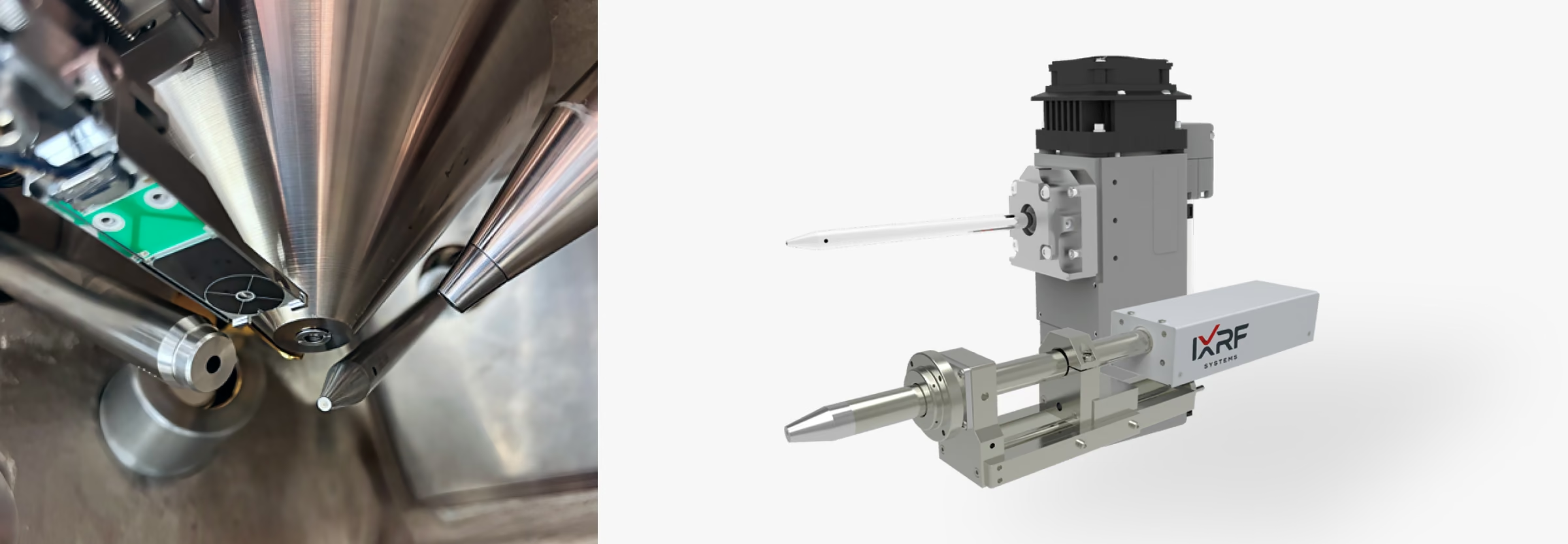
Most EDS systems use only the electron beam to generate X-rays from a sample. SEM/MicroXRF adds a second excitation source, an X-ray beam, which reaches deeper into the sample, covers a broader range of elements from sodium through uranium using K and L lines, and achieves trace-element sensitivity that EDS alone cannot match. IXRF's Xb micro-spot X-ray source fits on an unused high-angle port of almost any SEM. The two techniques complement each other: labs running both get more complete compositional data from a single instrument, without opening the chamber to switch methods.
Electron Beam and X-Ray Excitation Cover Different Ground
From 0 to 2 keV, electron-beam excitation (SEM/EDS) is clearly more efficient. Above about 2 keV, X-ray photon excitation (SEM/MicroXRF) becomes orders of magnitude more efficient, allowing quantification of more elements at lower concentrations than is possible with SEM/EDS alone. For matrices of lower mean atomic number, such as plastics, sensitivity is high enough to distinguish specimens differing by as little as 0.1 in mean atomic number.
Sensitivity
Higher peak-to-background ratios enable greater elemental sensitivity for higher-Z elements, exceeding SEM/EDS by a factor of 10 to 1000.
Precision
Extreme X-ray beam stability, paired with premium SDD detectors, yields the highest achievable precision and lowest detection limits.
Non-Destructive
Analyzes non-conductive materials without coating or electron-beam damage.
Hardware
The Xb Micro-Spot X-Ray Source
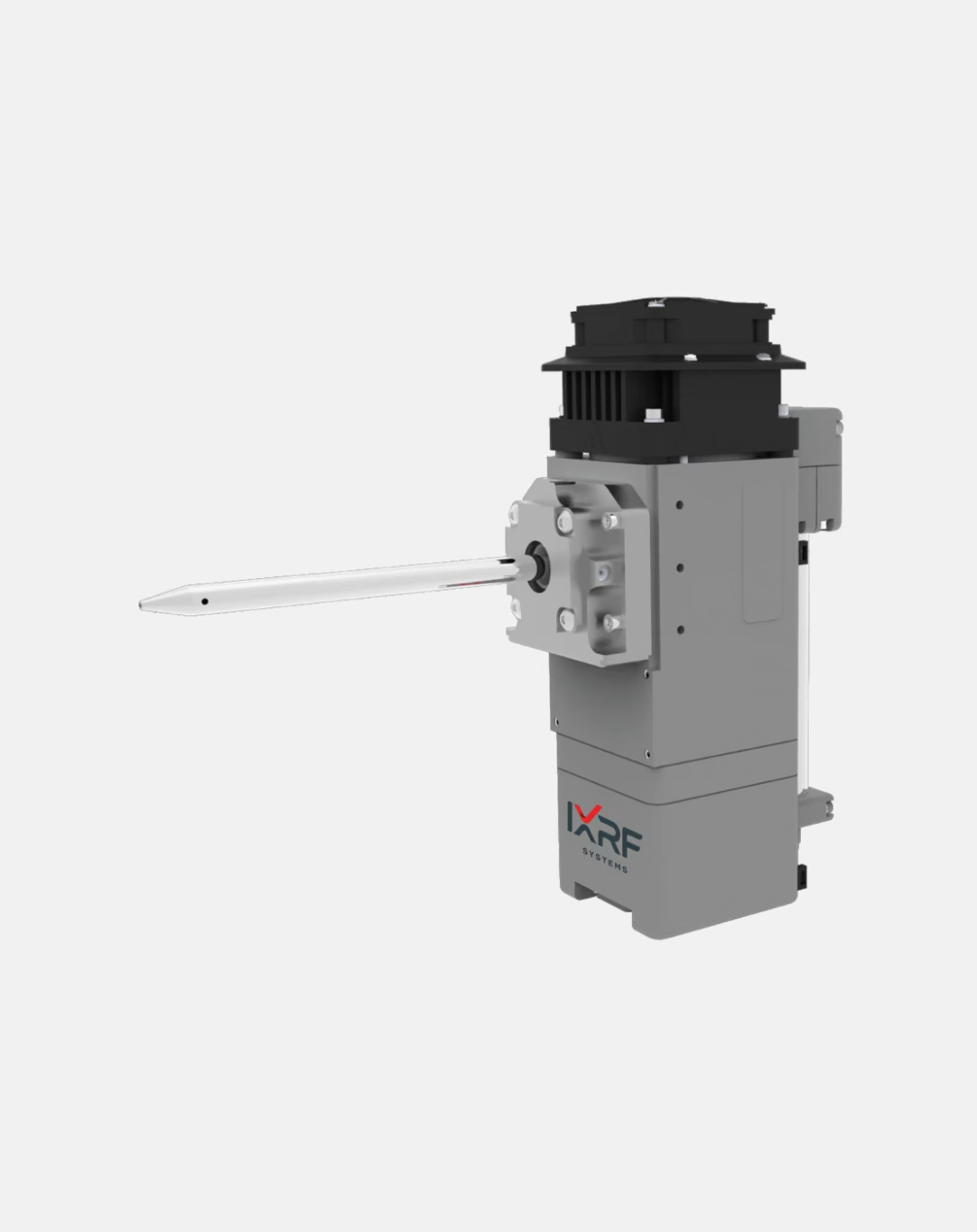
A compact design with slide mounting allows very close coupling to the sample. Patented polycapillary optics focus X-ray photons down to a spot size as small as 20 µm, with an integrated high-voltage power supply operating up to 50 W. Close coupling provides analytical results comparable to a traditional benchtop or mainframe XRF instrument, and the source does not interfere with normal electron microscope operation.
Software
Paired With Iridium Ultra Software
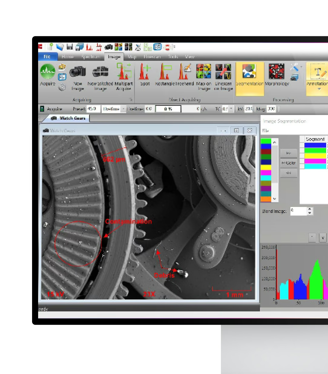
Every IXRF SEM/MicroXRF configuration runs on Iridium Ultra, IXRF's all-inclusive software suite for spectra, imaging, mapping, and linescans, so EDS and XRF data share one environment. Software upgrades are included for the life of the system, at no cost.
The ƒX SEM Source
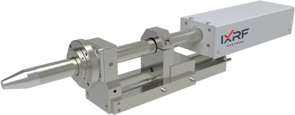
IXRF's ƒX SEM is an affordable X-ray source designed exclusively for electron microscopes, with the same close coupling and slide mounting as the Xb. It delivers high-flux X-rays to small or large excitation areas, and its integrated power supply operates up to 10 W without interfering with normal SEM operation.
Where SEM/MicroXRF Gets Used
Geology & Ore
Metal and ore characterization, and mineral and mineral-product analysis.
Coatings & Plating
Coatings, thin-film analysis, plating, and plating baths.
Forensics & Art
Art and archaeological analysis, and forensics.
Environmental
Environmental, food, and chemical applications.
Pharmaceutical & Cosmetic
Pharmaceutical applications and cosmetic analysis.
Plastics & Materials
Plastics, polymers, rubber, and concrete.
You Might Also Need
SEM/EDS
The electron-beam EDS platform that SEM/MicroXRF builds on, for any scanning electron microscope.
Atlas MicroXRF
A standalone microXRF spectrometer for full-sample mapping outside the SEM chamber.
EDS Software
Iridium Ultra: acquisition, quantification, mapping, and phase classification.
Frequently
Asked Questions
SEM-EDS uses the SEM’s electron beam to generate characteristic X-rays, while SEM-XRF uses a dedicated X-ray photon source for excitation. Photon excitation produces much lower spectral background for many higher-energy elements, improving trace-element sensitivity while complementing the high spatial resolution and light-element performance of SEM-EDS.
Adding XRF gives the SEM a second, complementary excitation method. SEM-XRF can provide substantially improved peak-to-background ratios and trace-element sensitivity for many medium- and high-energy elements, while EDS remains highly effective for microscopic features and lower-energy elements.
Yes. SEM-XRF is designed as an add-on for existing scanning electron microscopes and can operate alongside an installed EDS system. The X-ray source is typically mounted through an available SEM chamber port, subject to the microscope’s geometry and configuration.
The Xb uses polycapillary focusing optics for microXRF analysis, with focused spot sizes as small as 20 µm and higher source power (up to 50 W). The ƒX uses a compact end-window transmission source (up to 10 W) with larger excitation areas, from 200 µm upward, making it suitable when throughput or larger-area excitation matters more than micron-scale resolution.
SEM-XRF provides broad elemental coverage from approximately sodium (Na) through uranium (U). Combining X-ray excitation with SEM-EDS allows users to take advantage of electron excitation for lower-energy elements and X-ray excitation for sensitive analysis of medium- and higher-energy elements.
Yes. The lower spectral background produced by direct X-ray excitation can improve sensitivity for many trace elements that are difficult to distinguish using electron-beam excitation alone. SEM-XRF can also generate elemental maps showing the spatial distribution of these lower-concentration elements.
Yes. IXRF SEM-XRF supports simultaneous electron-beam and X-ray excitation at the same sample position. This enables complementary elemental information to be collected without moving the sample between the two excitation methods.
No. The SEM-XRF source is designed to remain in its measurement position without interfering with normal SEM operation. The electron beam can continue to be used on the same sample, including during simultaneous X-ray excitation workflows.
No. X-ray fluorescence does not require the sample to be electrically conductive, so nonconductive materials can be analyzed without conductive coating for the XRF measurement. This can be particularly useful for samples where coating could alter or obscure the original surface.
Yes. SEM-XRF supports quantitative elemental analysis using methods including Fundamental Parameters (FP), ZAF, least-squares, and standards-based approaches. XRF and EDS data can also be used together to provide complementary quantitative information across a broader elemental and energy range.
In many cases, yes. SEM-XRF sources are designed to interface with a wide range of SEM platforms using available high-angle or horizontal chamber ports. Compatibility depends on the specific microscope, available ports, chamber geometry, working distance, and detector configuration.
SEM-XRF is especially useful for applications requiring trace-element analysis, elemental mapping, thin-film or coating analysis, and characterization of nonconductive materials. Applications include geology and minerals, metals and alloys, electronics, coatings, environmental materials, glass, cultural heritage materials, powders, residues, and other complex materials.
Ready to See Beyond EDS?
Tell us your sample types and the elements you need to reach. We will recommend the Xb or ƒX configuration for your SEM.