Energy Dispersive X-Ray Spectroscopy for Any Scanning Electron Microscope
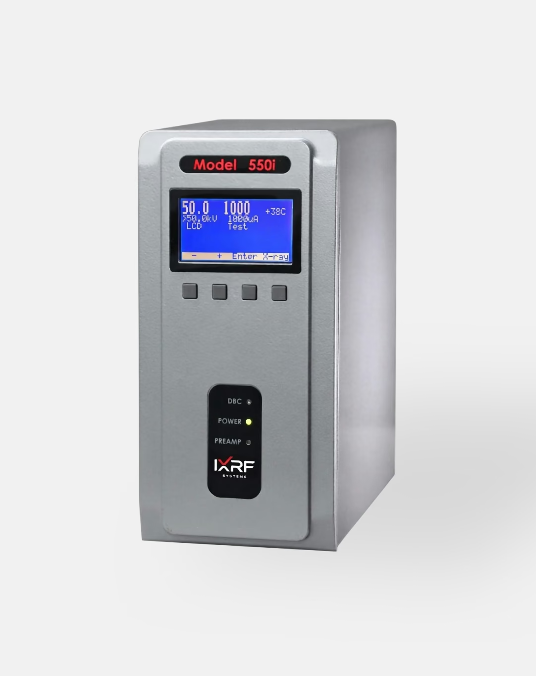
IXRF has spent two decades building EDS systems most vendors can't match, pairing SDD detectors with the Model 550i digital pulse processor to reach resolutions as tight as 123 eV.
Iridium Ultra, the software suite behind every spectrum, image, map, and linescan, comes standard — not licensed in tiers — and every upgrade for the life of the instrument is free.
When you're ready to see further, the same platform adds SEM-XRF with a polycapillary source, pushing sensitivity for higher-Z elements 10 to 1000× beyond what electron-beam excitation alone can reach.
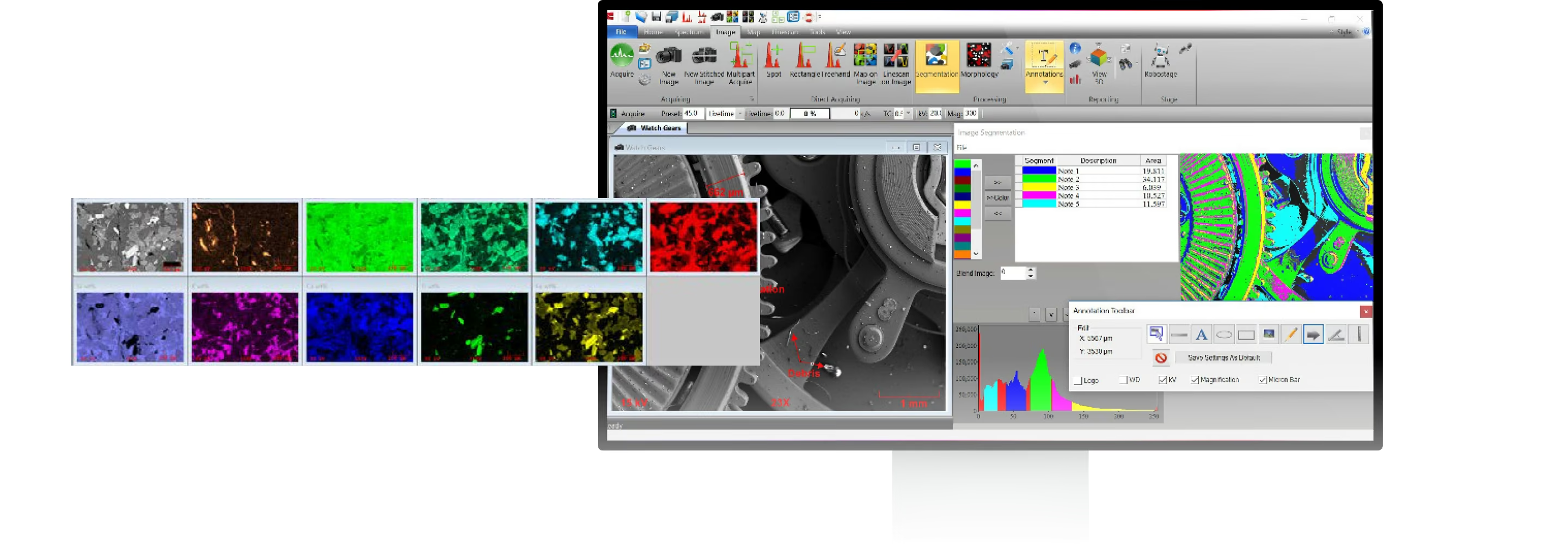
Over the past two decades, IXRF has proven itself as a leader in X-ray microanalysis
IXRF offers an all-inclusive software suite with a wide range of spectral, mapping, imaging, and automated analysis tools, couples only premium-quality detectors with every system, and provides free software upgrades for the life of the system. Energy-dispersive X-ray spectroscopy analyzes the X-rays generated when a focused electron beam strikes a sample inside an SEM: because each element emits X-rays at characteristic energies, the spectrum reveals which elements are present — and at what concentration — at the point of the beam or across a mapped area.
Hardware
Our Electronics Are Optimized for True Data Streaming and Ultra-Fast X-Ray Processing
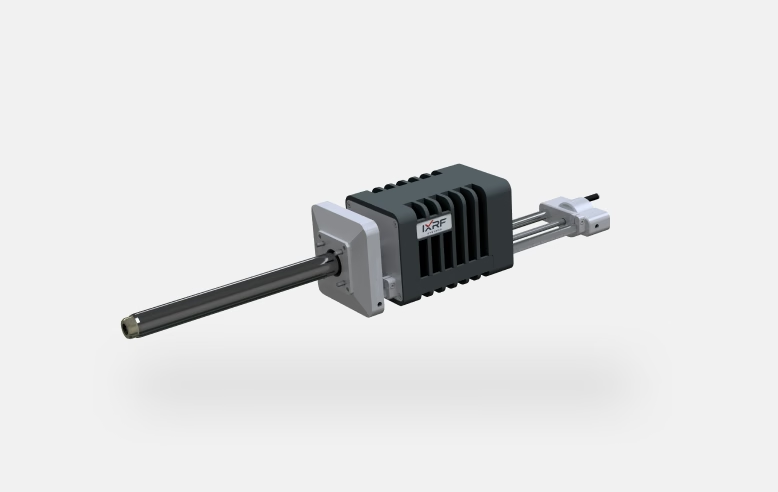
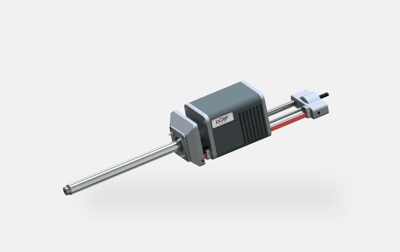
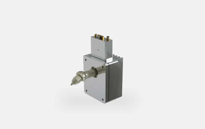
IXRF's range of electronically cooled (LN2-free) silicon drift detectors is optimized when coupled with an innovative Ethernet-based digital pulse processor. IXRF SDDs provide exceptional, stable performance over a wide range of input count rates.
Features:
- System incorporates Active Imaging combined with digital processing X-ray electronics
- 10/100 megabits/second Ethernet for easy adaptation to any PC networking system
- 4096 multi-channel analyzer
- CE certified, fully digital X-ray acquisition and detector control, with built-in liquid nitrogen warm-up protection when Si(Li) detectors are offered
- Data streaming: multiple buffers provide optimal mapping efficiency to support high count rate applications
- LCD display shows count rate, detector voltages and oscilloscope functions
Software
Iridium Ultra, and a Computer That Stays Current
IXRF can update your SEM/EDS software and computer to a current Windows environment, with Office interoperability for fast report generation and compliance with modern institutional security protocols. Software upgrades are included for the life of the system, at no cost.
What's in the System
- Detector
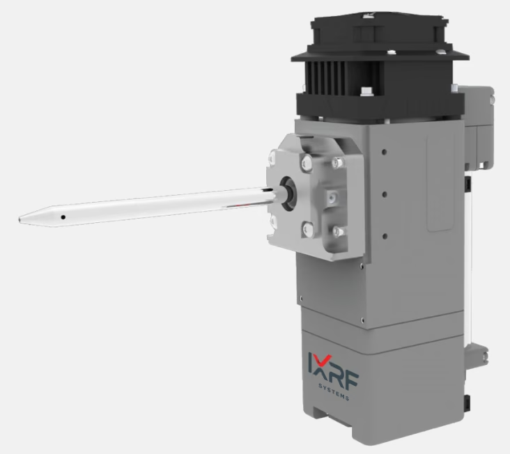
- Silicon drift detector (SDD), 10–100 mm² active area, vibration-free
- Window options
- Beryllium (8 µm) to thin polymer, for light-element X-ray transmission
- Electronics
- Model 550i digital pulse processor — Active Imaging, DSP, and 4096-channel MCA
- Cooling
- Electronically cooled (LN2-free)
- Software
- Iridium Ultra — free upgrades for the life of the system
- Upgrade path
- SEM-XRF: add a polycapillary X-ray source for 10–1000× higher-Z sensitivity
Upgrade Path
Add SEM-XRF for Higher-Z Sensitivity
Adding a polycapillary X-ray source and Iridium Ultra software transforms an existing SEM/EDS into a quantitative SEM-XRF system. Higher peak-to-background ratios boost sensitivity for higher-Z elements by a factor of 10–1000× over electron-beam excitation alone, without replacing the base EDS system.
One Software Suite, Four Workflows
Spectra, imaging, mapping, and linescans in one Iridium Ultra environment — included with every IXRF EDS system.
Spectra
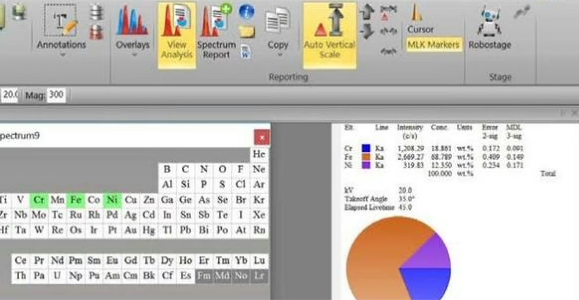
Identify, process, annotate, compare, and report spectra.
- Identifying elements — Kα energy markers and cursor ID
- Spectrum processing — Gaussian deconvolution, automatic peak-overlap correction, escape/sum peak removal, and standardless ZAF quantification
- Annotations — measure, label, and export directly on the spectrum
- Spectrum overlay — compare relative compositions across samples
- Spectrum reporting — one-click spreadsheet report of multiple spectra
Imaging
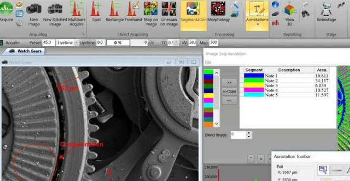
Acquire and analyze directly on the SEM image.
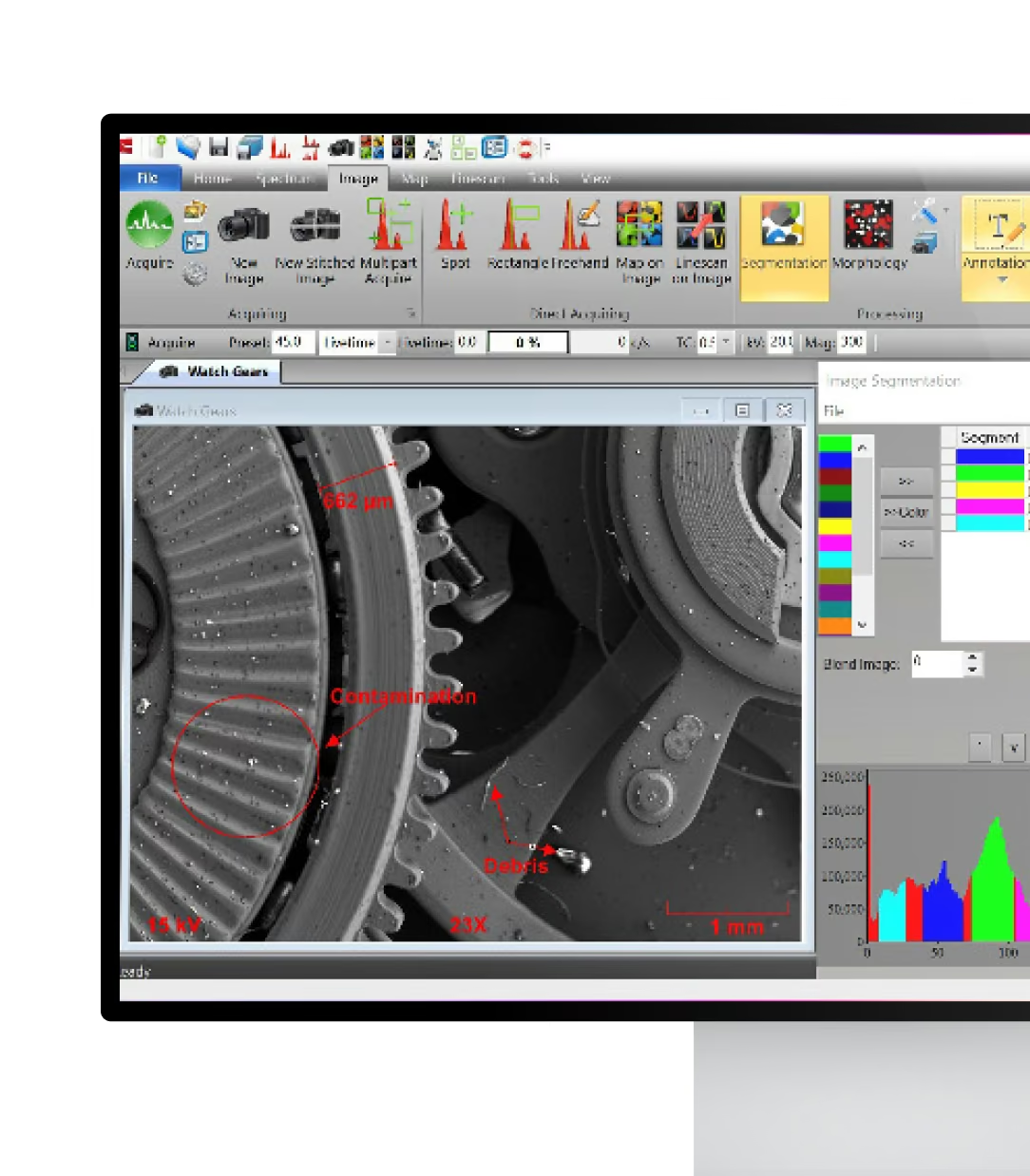
- Direct acquire — spot, rectangle, or freehand spectra, maps, and linescans on the SEM image
- Multipart acquire — automated analysis across points, raster areas, and freehand lines
- Segmentation — visual phase breakdown with percent-area histogram analysis
- Morphology — image binarization for particle area, perimeter, and shape data
- Stitching/montage and automated particle and multi-point analysis
Mapping
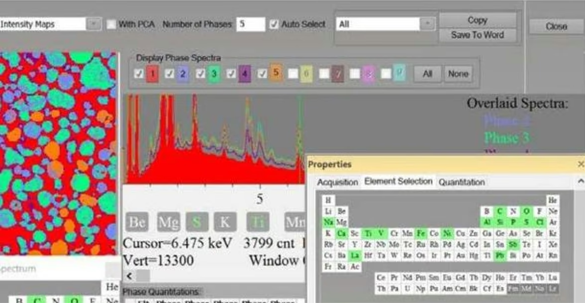
Quantitative, phase, and ratio maps with unattended acquisition.
- Multielement quantitative mapping, overlay maps, and composition mapping by custom compound
- Phase maps — automatic phase identification with phase-specific overlaid spectra
- Ratio maps — element weight-percent ratio comparison across a region
- Beam drift correction, maximum pixel spectrum, and map stitching and montage
- Automated stage and beam control for unattended acquisition
Linescans
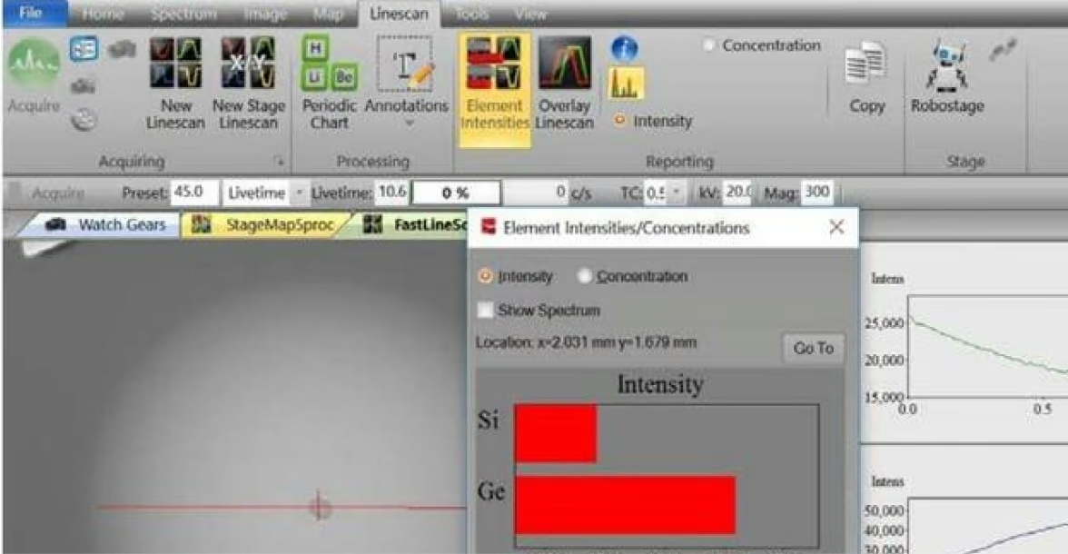
Profile composition along a line and compare scans directly.
- Multielement linescan acquisition
- Linescan overlay for direct comparison
- DataView — toggle between intensity and concentration
- MultiScan — stability control over long acquisitions
Where SEM/EDS Gets Used
Geology & Mining
Mineral identification, phase boundaries, rock structure, mining exploration, and test-core characterization.
Metals & Materials
Metals and alloys, corrosion analysis, wear and failure analysis, and RoHS/WEEE/ELV compliance.
Forensics
Glass chips, paint cross-sections, gunshot residue, and material identification for court-ready evidence.
Semiconductor & Electronics
Solder voids, X-ray imaging of PCBs, ion migration, defect analysis, and contaminant identification.
Biomedical & Pharma
Biomedical devices, implants, medical wear debris, and pathology.
Archaeology & Art
Archaeology, museums, artifacts, currency, gemstones, and paint and pigment analysis.
You Might Also Need
Atlas MicroXRF
Imaging spectrometer for full-sample mapping outside the SEM chamber.
SEM-XRF
X-ray sources that add microXRF capability to this system.
SDD Detectors
Replacement or upgrade detectors for SEM or TEM.
Not Sure Which Configuration Fits Your Samples?
Tell us your sample types and the resolution or sensitivity your lab requires. We will recommend the right SEM/EDS or SEM-XRF configuration.
Frequently
Asked Questions
IXRF offers electronically cooled silicon drift detectors with active areas from 10 mm² to 100 mm². The best detector depends on your SEM geometry, applications, desired count rate, light-element requirements, and analytical throughput.
A larger effective detector area can collect more X-rays, increasing count rate and potentially reducing acquisition time. However, actual performance also depends on detector position, solid angle, collimation, working distance, and the count-rate capability of the detector and electronics.
Yes. IXRF can replace an existing EDS system or upgrade compatible installations with new software, electronics, computers, and detectors. Existing functional detectors may also be retained while the electronics and software are modernized.
Yes. With the appropriate light-element detector window, IXRF SEM-EDS systems can detect light elements including B, C, N, O, and F, as well as transition metals and heavier elements. Actual performance depends on detector configuration, accelerating voltage, sample composition, and analytical conditions.
Energy resolution depends on detector active area and configuration. Current IXRF specifications place its SDD detector options in approximately the low-120s to low-130s eV range at Mn Kα, providing the spectral resolution needed to separate closely spaced elemental peaks.
SEM-EDS normally operates under the vacuum conditions required by the scanning electron microscope. Conductive samples generally require no coating, while nonconductive materials may require conductive coating, low-vacuum operation, or other preparation depending on the SEM and analytical objective.
Both techniques detect characteristic X-rays generated by an electron beam, but they operate in different microscopes. SEM-EDS is commonly used for surface and near-surface elemental analysis of bulk samples, while TEM-EDS analyzes electron-transparent specimens at much higher spatial resolution.
Yes. Ceramics, minerals, polymers, glasses, and other nonconductive materials can be analyzed by SEM-EDS. Depending on the microscope and sample, conductive coating, reduced accelerating voltage, or variable-pressure operation may be used to minimize charging.
IXRF SEM-EDS systems include Iridium Ultra, providing spectrum acquisition, automatic peak identification, quantitative analysis, elemental mapping, linescans, phase analysis, image processing, automation, and reporting within one software environment. IXRF currently includes software upgrades at no additional cost for the life of the system.
Yes. Iridium Ultra supports multi-element mapping, quantitative concentration maps, linescans, automated multi-point acquisition, phase analysis, map stitching, and standardless ZAF quantification. Automated workflows can also collect EDS data from multiple locations across the SEM stage.
A complete IXRF SEM-EDS package includes the SDD detector, digital signal-processing electronics, and Iridium Ultra acquisition and analysis software, configured for the customer’s SEM. Installation, system testing, and training can be incorporated into the system package.
IXRF typically needs the SEM manufacturer and model, available detector port, chamber and stage geometry, working distance, existing EDS hardware, and intended applications. This information allows the detector geometry and mounting configuration to be optimized for X-ray collection efficiency and sample clearance.